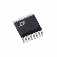
LTC2415-1CGN Linear Technology, LTC2415-1CGN Datasheet - Page 29

LTC2415-1CGN
Manufacturer Part Number
LTC2415-1CGN
Description
IC ADC 24BIT DIFFINPUT/REF16SSOP
Manufacturer
Linear Technology
Datasheet
1.LTC2415CGNPBF.pdf
(40 pages)
Specifications of LTC2415-1CGN
Number Of Bits
24
Sampling Rate (per Second)
13.75
Data Interface
MICROWIRE™, Serial, SPI™
Number Of Converters
2
Power Dissipation (max)
1mW
Voltage Supply Source
Single Supply
Operating Temperature
0°C ~ 70°C
Mounting Type
Surface Mount
Package / Case
16-SSOP (0.150", 3.90mm Width)
Lead Free Status / RoHS Status
Contains lead / RoHS non-compliant
Available stocks
Company
Part Number
Manufacturer
Quantity
Price
Company:
Part Number:
LTC2415-1CGN
Manufacturer:
LT
Quantity:
10 000
Part Number:
LTC2415-1CGN
Manufacturer:
LINEAR/凌特
Quantity:
20 000
Company:
Part Number:
LTC2415-1CGN#PBF
Manufacturer:
TI
Quantity:
120
Part Number:
LTC2415-1CGN#PBF
Manufacturer:
LINEAR/凌特
Quantity:
20 000
Part Number:
LTC2415-1CGN#TRPBF
Manufacturer:
LINEAR/凌特
Quantity:
20 000
APPLICATIO S I FOR ATIO
used for the external source impedance seen by IN
IN
gain errors will be insignificant (about 1% of their respec-
tive values over the entire temperature and voltage range).
Even for the most stringent applications, a one-time
calibration operation may be sufficient.
–
, the expected drift of the dynamic current, offset and
Figure 22. +FS Error vs R
300
240
180
120
60
0
0 100 200 300 400 500 600 700 800 900 1000
V
REF
REF
IN
IN
F
T
O
A
CC
+
–
U
= GND
= 25 C
+
–
= 3.75V
= 1.25V
= 5V
= 5V
= GND
U
SOURCE
R
SOURCE
Figure 24. Offset Error vs Common Mode Voltage
(V
( R
C
C
IN
IN
at IN
INCM
( )
= 0.01 F
= 1 F, 10 F
IN
C
W
IN
= R
+
= IN
= 0.1 F
or IN
SOURCEIN
+
= IN
2415 F22
–
–100
–120
120
100
–20
–40
–60
–80
(Large C
80
60
40
20
0
–
0 0.5 1 1.5 2 2.5 3 3.5 4 4.5 5
) and Input Source Resistance Imbalance
+ – R
A: R
B: R
C: R
D: R
U
IN
IN
IN
IN
A
B
C
D
E
F
G
SOURCEIN
IN
+
= +400
= +200
= +100
= 0
)
and
V
REF
REF
IN
F
T
R
C
CC
+
O
A
IN
SOURCEIN
V
+
–
= IN
= GND
–) for Large C
= 5V
= 25 C
= 10 F
INCM
= 5V
= GND
In addition to the input sampling charge, the input ESD
protection diodes have a temperature dependent leakage
current. This current, nominally 1nA ( 10nA max), results
in a small offset shift. A 100 source resistance will create
a 0.1 V typical and 1 V maximum offset voltage.
–
= V
(V)
– = 500
INCM
Figure 23. –FS Error vs R
E: R
F: R
G: R
IN
IN
IN
= –200
= –100
IN
= –400
Values (C
–120
–180
–240
–300
2415 F24
–60
0
0 100 200 300 400 500 600 700 800 900 1000
LTC2415/LTC2415-1
V
REF
REF
IN
IN
F
T
O
A
CC
+
–
= GND
= 25 C
IN
+
–
= 1.25V
= 3.75V
= 5V
= 5V
= GND
1 F)
SOURCE
R
SOURCE
C
IN
at IN
( )
= 1 F, 10 F
C
C
IN
IN
+
= 0.01 F
= 0.1 F
or IN
2415 F23
–
(Large C
sn2415 24151fs
29
IN
)


