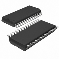
LTC1419AISW#PBF Linear Technology, LTC1419AISW#PBF Datasheet - Page 11

LTC1419AISW#PBF
Manufacturer Part Number
LTC1419AISW#PBF
Description
IC A/D CONV 14BIT SAMPLNG 28SOIC
Manufacturer
Linear Technology
Datasheet
1.LTC1419ACG.pdf
(20 pages)
Specifications of LTC1419AISW#PBF
Number Of Bits
14
Sampling Rate (per Second)
800k
Data Interface
Parallel
Number Of Converters
1
Power Dissipation (max)
240mW
Voltage Supply Source
Dual ±
Operating Temperature
-40°C ~ 85°C
Mounting Type
Surface Mount
Package / Case
28-SOIC (0.300", 7.50mm Width)
Lead Free Status / RoHS Status
Lead free / RoHS Compliant
Available stocks
Company
Part Number
Manufacturer
Quantity
Price
APPLICATIONS
many applications. For example, Figure 7 shows a 1000pF
capacitor from + A
to limit the input bandwidth to 1.6MHz. The 1000pF
capacitor also acts as a charge reservoir for the input
sample-and-hold and isolates the ADC input from sam-
pling glitch sensitive circuitry. High quality capacitors and
resistors should be used since these components can add
distortion. NPO and silver mica type dielectric capacitors
have excellent linearity. Carbon surface mount resistors can
also generate distortion from self heating and from damage
that may occur during soldering. Metal film surface mount
resistors are much less susceptible to both problems.
Input Range
The ±2.5V input range of the LTC1419 is optimized for low
noise and low distortion. Most op amps also perform well
over this same range, allowing direct coupling to the
analog inputs and eliminating the need for special transla-
tion circuitry.
Some applications may require other input ranges. The
LTC1419 differential inputs and reference circuitry can
accommodate other input ranges often with little or no
additional circuitry. The following sections describe the
reference and input circuitry and how they affect the input
range.
Internal Reference
The LTC1419 has an on-chip, temperature compensated,
curvature corrected, bandgap reference that is factory
trimmed to 2.500V. It is connected internally to a reference
amplifier and is available at V
4.0625V
2.500V
10µF
Figure 8a. LTC1419 Reference Circuit
3
4
5
V
REFCOMP
AGND
REF
IN
U
to ground and a 100Ω source resistor
INFORMATION
64k
R3
U
REFERENCE
40k
R2
REF
AMP
(Pin 3) see Figure 8a. A
W
R1
2k
REFERENCE
BANDGAP
LTC1419
U
1419 F08a
2k resistor is in series with the output so that it can be
easily overdriven by an external reference or other
circuitry, see Figure 8b. The reference amplifier gains the
voltage at the V
internal reference voltage. This provides buffering be-
tween the V
reference amplifier compensation pin (REFCOMP, Pin 4)
must be bypassed with a capacitor to ground. The refer-
ence amplifier is stable with capacitors of 1µF or greater.
For the best noise performance, a 10µF ceramic or 10µF
tantalum in parallel with a 0.1µF ceramic is recommended.
The V
shown in Figure 9. This is useful in applications where the
peak input signal amplitude may vary. The input span of
the ADC can then be adjusted to match the peak input
signal, maximizing the signal-to-noise ratio. The filtering
of the internal LTC1419 reference amplifier will limit the
bandwidth and settling time of this circuit. A settling time
of 5ms should be allowed for after a reference adjustment.
Figure 8b. Using the LT1019-2.5 as an External Reference
REF
LT1019A-2.5
pin can be driven with a DAC or other means
REF
LTC1450
V
5V
IN
Figure 9. Driving V
pin and the high speed capacitive DAC. The
V
OUT
REF
+
pin by 1.625 to create the required
10µF
ANALOG
ANALOG INPUT
DIFFERENTIAL
INPUT
1.25V TO 3V
1.25V TO 3V
10µF
0.1µF
REF
1
2
3
4
5
with a DAC
+A
–A
V
REFCOMP
AGND
1
2
3
4
5
REF
IN
IN
+A
–A
V
REFCOMP
AGND
LTC1419
REF
IN
IN
LTC1419
LTC1419
1419 F08b
1419 F09
11
1419fb


