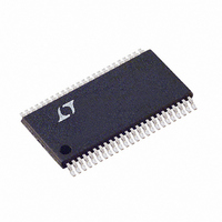
LTC1750IFW Linear Technology, LTC1750IFW Datasheet - Page 12

LTC1750IFW
Manufacturer Part Number
LTC1750IFW
Description
IC ADC 14BIT 80MSPS SMPL 48TSSOP
Manufacturer
Linear Technology
Datasheet
1.LTC1750CFW.pdf
(20 pages)
Specifications of LTC1750IFW
Number Of Bits
14
Sampling Rate (per Second)
80M
Data Interface
Parallel
Number Of Converters
1
Power Dissipation (max)
1.69W
Voltage Supply Source
Single Supply
Operating Temperature
-40°C ~ 85°C
Mounting Type
Surface Mount
Package / Case
48-TFSOP (0.240", 6.10mm Width)
Lead Free Status / RoHS Status
Contains lead / RoHS non-compliant
Available stocks
Company
Part Number
Manufacturer
Quantity
Price
Part Number:
LTC1750IFW#PBF
Manufacturer:
LINEAR/凌特
Quantity:
20 000
APPLICATIO S I FOR ATIO
LTC1750
In operation, the ADC quantizes the input to the stage and
the quantized value is subtracted from the input by the
DAC to produce a residue. The residue is amplified and
output by the residue amplifier. Successive stages operate
out of phase so that when the odd stages are outputting
their residue, the even stages are acquiring that residue
and visa versa.
When ENC is low, the analog input is sampled differentially
directly onto the input sample-and-hold capacitors, inside
the “Input S/H” shown in the block diagram. At the instant
that ENC transitions from low to high, the sampled input
is held. While ENC is high, the held input voltage is
buffered by the S/H amplifier which drives the first pipelined
ADC stage. The first stage acquires the output of the S/H
during this high phase of ENC. When ENC goes back low,
the first stage produces its residue which is acquired by
the second stage. At the same time, the input S/H goes
back to acquiring the analog input. When ENC goes back
high, the second stage produces its residue which is
acquired by the third stage. An identical process is re-
peated for the third stage, resulting in a third stage residue
that is sent to the fourth stage ADC for final evaluation.
Each ADC stage following the first has additional range to
accommodate flash and amplifier offset errors. Results
from all of the ADC stages are digitally synchronized such
that the results can be properly combined in the correction
logic before being sent to the output buffer.
SAMPLE/HOLD OPERATION AND INPUT DRIVE
Sample/Hold Operation
Figure 2 shows an equivalent circuit for the LTC1750
CMOS differential sample-and-hold. The differential ana-
log inputs are sampled directly onto sampling capacitors
(C
sampling results in lowest possible noise for a given
sampling capacitor size. The capacitors shown attached to
each input (C
capacitance associated with each input.
During the sample phase when ENC/ENC is low, the NMOS
switch connects the analog inputs to the sampling capaci-
tors and they charge to, and track the differential input
voltage. When ENC/ENC transitions from low to high the
12
SAMPLE
) through NMOS switches. This direct capacitor
PARASITIC
U
) are the summation of all other
U
W
U
sampled input voltage is held on the sampling capacitors.
During the hold phase when ENC/ENC is high the sampling
capacitors are disconnected from the input and the held
voltage is passed to the ADC core for processing. As
ENC/ENC transitions from high to low the inputs are
reconnected to the sampling capacitors to acquire a new
sample. Since the sampling capacitors still hold the previ-
ous sample, a charging glitch proportional to the change
in voltage between samples will be seen at this time. If the
change between the last sample and the new sample is
small the charging glitch seen at the input will be small. If
the input change is large, such as the change seen with
input frequencies near Nyquist, then a larger charging
glitch will be seen.
Common Mode Bias
The ADC sample-and-hold circuit requires differential drive
to achieve specified performance. Each input should swing
within the valid input range, around a common mode volt-
age of 2.0V. The V
vide the common mode bias level. V
to the center tap of a transformer to set the DC input level
or as a reference level to an op amp differential driver cir-
cuit. The V
ADC with a 4.7 F or greater capacitor.
A
A
ENC
ENC
IN
IN
+
–
LTC1750
V
V
2V
2V
DD
DD
CM
6k
6k
pin must be bypassed to ground close to the
5V
Figure 2. Equivalent Input Circuit
CM
C
2.4pF
C
2.4pF
output pin (Pin 2) may be used to pro-
PARASITIC
PARASITIC
BIAS
30
30
R
R
ON
ON
CM
can be tied directly
C
1pF
C
1pF
PARASITIC
PARASITIC
C
C
SAMPLE
SAMPLE
3.5pF
3.5pF
1750 F02
1750f


