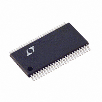
LTC1750IFW Linear Technology, LTC1750IFW Datasheet - Page 17

LTC1750IFW
Manufacturer Part Number
LTC1750IFW
Description
IC ADC 14BIT 80MSPS SMPL 48TSSOP
Manufacturer
Linear Technology
Datasheet
1.LTC1750CFW.pdf
(20 pages)
Specifications of LTC1750IFW
Number Of Bits
14
Sampling Rate (per Second)
80M
Data Interface
Parallel
Number Of Converters
1
Power Dissipation (max)
1.69W
Voltage Supply Source
Single Supply
Operating Temperature
-40°C ~ 85°C
Mounting Type
Surface Mount
Package / Case
48-TFSOP (0.240", 6.10mm Width)
Lead Free Status / RoHS Status
Contains lead / RoHS non-compliant
Available stocks
Company
Part Number
Manufacturer
Quantity
Price
Part Number:
LTC1750IFW#PBF
Manufacturer:
LINEAR/凌特
Quantity:
20 000
APPLICATIO S I FOR ATIO
Output Loading
As with all high speed/high resolution converters the
digital output loading can affect the performance. The
digital outputs of the LTC1750 should drive a minimal
capacitive load to avoid possible interaction between the
digital outputs and sensitive input circuitry. The output
should be buffered with a device such as an ALVCH16373
CMOS latch. For full speed operation the capacitive load
should be kept under 10pF. A resistor in series with the
output may be used but is not required since the ADC has
a series resistor of 43 on chip.
Lower OV
from the digital outputs.
Format
The LTC1750 parallel digital output can be selected for
offset binary or 2’s complement format. The format is
selected with the MSBINV pin; high selects offset binary.
Overflow Bit
An overflow output bit indicates when the converter is
overranged or underranged. When OF outputs a logic high
the converter is either overranged or underranged.
Output Clock
The ADC has a delayed version of the ENC input available
as a digital output, CLKOUT. The CLKOUT pin can be used
to synchronize the converter data to the digital system.
This is necessary when using a sinusoidal encode signal.
DD
voltages will also help reduce interference
U
U
LATCH
FROM
DATA
W
Figure 9. Equivalent Circuit for a Digital Output Buffer
PREDRIVER
LOGIC
V
DD
U
V
DD
Data will be updated just after CLKOUT falls and can be
latched on the rising edge of CLKOUT.
Output Driver Power
Separate output power and ground pins allow the output
drivers to be isolated from the analog circuitry. The power
supply for the digital output buffers, OV
to the same power supply as for the logic being driven. For
example if the converter is driving a DSP powered by a 3V
supply then OV
OV
outputs will swing between OGND and OV
GROUNDING AND BYPASSING
The LTC1750 requires a printed circuit board with a clean
unbroken ground plane. A multilayer board with an inter-
nal ground plane is recommended. The pinout of the
LTC1750 has been optimized for a flowthrough layout so
that the interaction between inputs and digital outputs is
minimized. Layout for the printed circuit board should
ensure that digital and analog signal lines are separated as
much as possible. In particular, care should be taken not
to run any digital track alongside an analog signal track or
underneath the ADC.
High quality ceramic bypass capacitors should be used at
the V
shown in the block diagram on the front page of this data
sheet. Bypass capacitors must be located as close to the
pins as possible. Of particular importance are the capaci-
tors between REFHA and REFLB and between REFHB and
DD
DD,
OV
can be powered with any voltage up to 5V. The logic
DD
V
LTC1750
CM
43
, REFHA, REFHB, REFLA and REFLB pins as
1750 F09
DD
OV
OGND
should be tied to that same 3V supply.
DD
0.1 F
0.5V TO
V
TYPICAL
DATA
OUTPUT
DD
DD
LTC1750
, should be tied
DD
.
17
1750f


