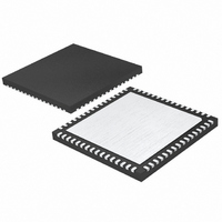
LTC2208CUP#TR Linear Technology, LTC2208CUP#TR Datasheet - Page 23

LTC2208CUP#TR
Manufacturer Part Number
LTC2208CUP#TR
Description
IC ADC 16BIT 130MSPS 64-QFN
Manufacturer
Linear Technology
Datasheet
1.LTC2208CUPPBF.pdf
(32 pages)
Specifications of LTC2208CUP#TR
Number Of Bits
16
Sampling Rate (per Second)
130M
Data Interface
Parallel
Number Of Converters
1
Power Dissipation (max)
1.78W
Voltage Supply Source
Single Supply
Operating Temperature
0°C ~ 70°C
Mounting Type
Surface Mount
Package / Case
64-WFQFN, Exposed Pad
Lead Free Status / RoHS Status
Contains lead / RoHS non-compliant
Available stocks
Company
Part Number
Manufacturer
Quantity
Price
APPLICATIONS INFORMATION
output may be used but is not required since the ADC has
a series resistor of 43Ω on chip.
Lower OV
from the digital outputs.
Digital Output Buffers (LVDS Modes)
Figure 12 shows an equivalent circuit for an LVDS output
pair. A 3.5mA current is steered from OUT
vice versa, which creates a ±350mV differential voltage
across the 100Ω termination resistor at the LVDS receiver.
A feedback loop regulates the common mode output volt-
age to 1.20V. For proper operation each LVDS output pair
must be terminated with an external 100Ω termination
LATCH
FROM
DATA
Figure 11. Equivalent Circuit for a Digital Output Buffer
PREDRIVER
LOGIC
DD
V
DD
voltages will also help reduce interference
LATCH
LTC2208
FROM
DATA
V
DD
PREDRIVER
LOGIC
V
DD
OV
Figure 12. Equivalent Output Buffer in LVDS Mode
DD
LTC2208
43Ω
2208 F11
+
to OUT
OV
OGND
10k
DD
1.20V
TYPICAL
DATA
OUTPUT
0.5V
TO 3.6V
0.1μF
V
–
DD
or
+
–
3.5mA
10k
resistor, even if the signal is not used (such as OF
CLKOUT
traces for each LVDS output pair should be routed close
together. To minimize clock skew all LVDS PC board traces
should have about the same length.
In Low Power LVDS Mode 1.75mA is steered between
the differential outputs, resulting in ±175mV at the LVDS
receiver’s 100Ω termination resistor. The output com-
mon mode voltage is 1.20V, the same as standard LVDS
Mode.
Data Format
The LTC2208 parallel digital output can be selected for
offset binary or 2’s complement format. The format is
selected with the MODE pin. This pin has a four level
logic input, centered at 0, 1/3V
external resistor divider can be user to set the 1/3V
and 2/3V
for the MODE pin.
Table 2. MODE Pin Function
0(GND)
1/3VDD
2/3VDD
OV
MODE
VDD
DD
OV
+
DD
DD
/CLKOUT
43Ω
43Ω
logic levels. Table 2 shows the logic states
2208 F12
100Ω
OGND
–
OUTPUT FORMAT
). To minimize noise the PC board
2’s Complement
2’s Complement
Offset Binary
Offset Binary
RECEIVER
OV
3.3V
0.1μF
LVDS
DD
DD
, 2/3V
LTC2208
CYCLE STABILIZER
DD
CLOCK DUTY
and V
Off
Off
On
On
+
23
/OF
DD
. An
2208fc
–
DD
or


