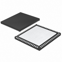
LTC2208CUP#TR Linear Technology, LTC2208CUP#TR Datasheet - Page 7

LTC2208CUP#TR
Manufacturer Part Number
LTC2208CUP#TR
Description
IC ADC 16BIT 130MSPS 64-QFN
Manufacturer
Linear Technology
Datasheet
1.LTC2208CUPPBF.pdf
(32 pages)
Specifications of LTC2208CUP#TR
Number Of Bits
16
Sampling Rate (per Second)
130M
Data Interface
Parallel
Number Of Converters
1
Power Dissipation (max)
1.78W
Voltage Supply Source
Single Supply
Operating Temperature
0°C ~ 70°C
Mounting Type
Surface Mount
Package / Case
64-WFQFN, Exposed Pad
Lead Free Status / RoHS Status
Contains lead / RoHS non-compliant
Available stocks
Company
Part Number
Manufacturer
Quantity
Price
ELECTRICAL CHARACTERISTICS
Note 1: Stresses beyond those listed under Absolute Maximum Ratings
may cause permanent damage to the device. Exposure to any Absolute
Maximum Rating condition for extended periods may affect device
reliability and lifetime.
Note 2: All voltage values are with respect to GND, with GND and OGND
shorted (unless otherwise noted).
Note 3: When these pin voltages are taken below GND or above V
will be clamped by internal diodes. This product can handle input currents
of greater than 100mA below GND or above V
Note 4: V
ENC
with differential drive (PGA = 0), unless otherwise specifi ed.
TIMING DIAGRAMS
–
= 2V
DD
P-P
= 3.3V, f
sine wave with 1.6V common mode, input range = 2.25V
SAMPLE
D0-D15, OF
CLKOUT
CLKOUT
ANALOG
INPUT
ENC
ENC
= 130MHz, LVDS outputs, differential ENC
–
+
+
–
N
DD
t
H
without latchup.
All Outputs are Differential and Have LVDS Levels
t
t
t
AP
D
C
N – 7
t
L
N + 1
LVDS Output Mode Timing
DD
N – 6
, they
P-P
+
/
N + 2
Note 5: Integral nonlinearity is defi ned as the deviation of a code from a “best
fi t straight line” to the transfer curve. The deviation is measured from the
center of the quantization band.
Note 6: Offset error is the offset voltage measured from –1/2LSB when the
output code fl ickers between 0000 0000 0000 0000 and 1111 1111 1111
1111 in 2’s complement output mode.
Note 7: Guaranteed by design, not subject to test.
Note 8: Recommended operating conditions.
N – 5
N + 3
N – 4
N – 3
N + 4
2208 TD01
LTC2208
2208fc
7


