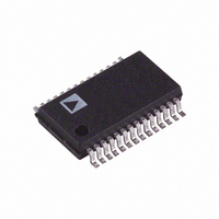
AD9200ARSRL Analog Devices Inc, AD9200ARSRL Datasheet - Page 23

AD9200ARSRL
Manufacturer Part Number
AD9200ARSRL
Description
IC ADC 10BIT CMOS 20MSPS 28-SSOP
Manufacturer
Analog Devices Inc
Datasheet
1.AD9200ARSZRL.pdf
(24 pages)
Specifications of AD9200ARSRL
Rohs Status
RoHS non-compliant
Number Of Bits
10
Sampling Rate (per Second)
20M
Data Interface
Parallel
Number Of Converters
9
Power Dissipation (max)
100mW
Voltage Supply Source
Single Supply
Operating Temperature
-40°C ~ 85°C
Mounting Type
Surface Mount
Package / Case
28-SSOP (0.200", 5.30mm Width)
GROUNDING AND LAYOUT RULES
As is the case for any high performance device, proper ground-
ing and layout techniques are essential in achieving optimal
performance. The analog and digital grounds on the AD9200
have been separated to optimize the management of return
currents in a system. Grounds should be connected near the
ADC. It is recommended that a printed circuit board (PCB) of
at least four layers, employing a ground plane and power planes,
be used with the AD9200. The use of ground and power planes
offers distinct advantages:
1. The minimization of the loop area encompassed by a signal
2. The minimization of the impedance associated with ground
3. The inherent distributed capacitor formed by the power plane,
These characteristics result in both a reduction of electro-
magnetic interference (EMI) and an overall improvement in
performance.
It is important to design a layout that prevents noise from cou-
pling onto the input signal. Digital signals should not be run in
parallel with the input signal traces and should be routed away
from the input circuitry. Separate analog and digital grounds
should be joined together directly under the AD9200 in a solid
ground plane. The power and ground return currents must be
carefully managed. A general rule of thumb for mixed signal
layouts dictates that the return currents from digital circuitry
should not pass through critical analog circuitry.
REV. E
and its return path.
and power paths.
PCB insulation and ground plane.
–23–
DIGITAL OUTPUTS
Each of the on-chip buffers for the AD9200 output bits
(D0–D9) is powered from the DRVDD supply pins, separate
from AVDD. The output drivers are sized to handle a variety
of logic families while minimizing the amount of glitch energy
generated. In all cases, a fan-out of one is recommended to keep
the capacitive load on the output data bits below the specified
20 pF level.
For DRVDD = 5 V, the AD9200 output signal swing is compat-
ible with both high speed CMOS and TTL logic families. For
TTL, the AD9200 on-chip, output drivers were designed to
support several of the high speed TTL families (F, AS, S). For
applications where the clock rate is below 20 MSPS, other TTL
families may be appropriate. For interfacing with lower voltage
CMOS logic, the AD9200 sustains 20 MSPS operation with
DRVDD = 3 V. In all cases, check your logic family data sheets
for compatibility with the AD9200 Digital Specification table.
THREE-STATE OUTPUTS
The digital outputs of the AD9200 can be placed in a high
impedance state by setting the THREE-STATE pin to HIGH.
This feature is provided to facilitate in-circuit testing or evaluation.
AD9200


