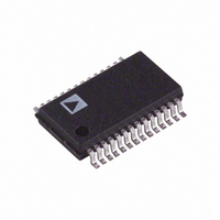
AD9200ARSRL Analog Devices Inc, AD9200ARSRL Datasheet - Page 9

AD9200ARSRL
Manufacturer Part Number
AD9200ARSRL
Description
IC ADC 10BIT CMOS 20MSPS 28-SSOP
Manufacturer
Analog Devices Inc
Datasheet
1.AD9200ARSZRL.pdf
(24 pages)
Specifications of AD9200ARSRL
Rohs Status
RoHS non-compliant
Number Of Bits
10
Sampling Rate (per Second)
20M
Data Interface
Parallel
Number Of Converters
9
Power Dissipation (max)
100mW
Voltage Supply Source
Single Supply
Operating Temperature
-40°C ~ 85°C
Mounting Type
Surface Mount
Package / Case
28-SSOP (0.200", 5.30mm Width)
SUMMARY OF MODES
VOLTAGE REFERENCE
1 V Mode the internal reference may be set to 1 V by connect-
ing REFSENSE and VREF together.
2 V Mode the internal reference my be set to 2 V by connecting
REFSENSE to analog ground
External Divider Mode the internal reference may be set to a
point between 1 V and 2 V by adding external resistors. See
Figure 16f.
External Reference Mode enables the user to apply an exter-
nal reference to REFTS, REFBS and VREF pins. This mode
is attained by tying REFSENSE to VDD.
REFERENCE BUFFER
Center Span Mode midscale is set by shorting REFTS and
REFBS together and applying the midscale voltage to that point
The MODE pin is set to AVDD/2. The analog input will swing
about that midscale point.
Top/Bottom Mode sets the input range between two points.
The two points are between 1 V and 2 V apart. The Top/Bottom
Mode is enabled by tying the MODE pin to AVDD.
ANALOG INPUT
Differential Mode is attained by driving the AIN pin as one
differential input and shorting REFTS and REFBS together and
driving them as the second differential input. The MODE pin
is tied to AVDD/2. Preferred mode for optimal distortion
performance.
Single-Ended is attained by driving the AIN pin while the
REFTS and REFBS pins are held at dc points. The MODE pin is
tied to AVDD.
Single-Ended/Clamped (AC Coupled) the input may be
clamped to some dc level by ac coupling the input. This is done
by tying the CLAMPIN to some dc point and applying a pulse
to the CLAMP pin. MODE pin is tied to AVDD.
SPECIAL
AD876 Mode enables users of the AD876 to drop the AD9200
into their socket. This mode is attained by floating or grounding
the MODE pin.
INPUT AND REFERENCE OVERVIEW
Figure 16, a simplified model of the AD9200, highlights the
relationship between the analog input, AIN, and the reference
voltages, REFTS, REFBS and VREF. Like the voltages applied
to the resistor ladder in a flash A/D converter, REFTS and
REFBS define the maximum and minimum input voltages to
the A/D.
The input stage is normally configured for single-ended opera-
tion, but allows for differential operation by shorting REFTS
and REFBS together to be used as the second input.
REV. E
–9–
In single-ended operation, the input spans the range,
where REFBS can be connected to GND and REFTS con-
nected to VREF. If the user requires a different reference range,
REFBS and REFTS can be driven to any voltage within the
power supply rails, so long as the difference between the two is
between 1 V and 2 V.
In differential operation, REFTS and REFBS are shorted to-
gether, and the input span is set by VREF,
where VREF is determined by the internal reference or brought
in externally by the user.
The best noise performance may be obtained by operating the
AD9200 with a 2 V input range. The best distortion perfor-
mance may be obtained by operating the AD9200 with a 1 V
input range.
REFERENCE OPERATION
The AD9200 can be configured in a variety of reference topolo-
gies. The simplest configuration is to use the AD9200’s onboard
bandgap reference, which provides a pin-strappable option to
generate either a 1 V or 2 V output. If the user desires a refer-
ence voltage other than those two, an external resistor divider
can be connected between VREF, REFSENSE and analog
ground to generate a potential anywhere between 1 V and 2 V.
Another alternative is to use an external reference for designs
requiring enhanced accuracy and/or drift performance. A
third alternative is to bring in top and bottom references,
bypassing VREF altogether.
Figures 16d, 16e and 16f illustrate the reference and input ar-
chitecture of the AD9200. In tailoring a desired arrangement,
the user can select an input configuration to match drive circuit.
Then, moving to the reference modes at the bottom of the
figure, select a reference circuit to accommodate the offset and
amplitude of a full-scale signal.
Table I outlines pin configurations to match user requirements.
Figure 15. AD9200 Equivalent Functional Input Circuit
(REFTS – VREF/2)
REFBS
REFTS
AIN
REFBS
AIN
AIN
SHA
AD9200
(REFTS + VREF/2)
REFTS
CORE
A/D
AD9200


