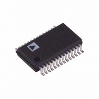
AD9201ARS Analog Devices Inc, AD9201ARS Datasheet - Page 3

AD9201ARS
Manufacturer Part Number
AD9201ARS
Description
IC ADC CMOS 10BIT DUAL 28-SSOP
Manufacturer
Analog Devices Inc
Specifications of AD9201ARS
Mounting Type
Surface Mount
Rohs Status
RoHS non-compliant
Number Of Bits
10
Sampling Rate (per Second)
20M
Data Interface
Parallel
Number Of Converters
2
Power Dissipation (max)
245mW
Voltage Supply Source
Analog and Digital
Operating Temperature
-40°C ~ 85°C
Package / Case
28-SSOP (0.200", 5.30mm Width)
Input Channels Per Adc
2
No. Of Channels
2
Peak Reflow Compatible (260 C)
No
Inl ±
2.5LSB
Sample Rate
20MSPS
No. Of Bits
10 Bit
Leaded Process Compatible
No
Dnl±
1LSB
Number Of Elements
2
Resolution
10Bit
Architecture
Pipelined
Input Polarity
Unipolar
Input Type
Voltage
Rated Input Volt
1.5V
Differential Input
Yes
Power Supply Requirement
Analog and Digital
Single Supply Voltage (typ)
3V
Single Supply Voltage (min)
2.7V
Single Supply Voltage (max)
5.5V
Dual Supply Voltage (typ)
Not RequiredV
Dual Supply Voltage (min)
Not RequiredV
Dual Supply Voltage (max)
Not RequiredV
Differential Linearity Error
±1LSB
Integral Nonlinearity Error
±2.5LSB
Operating Temp Range
-40C to 85C
Operating Temperature Classification
Industrial
Mounting
Surface Mount
Pin Count
28
Package Type
SSOP
Lead Free Status / Rohs Status
Not Compliant
Available stocks
Company
Part Number
Manufacturer
Quantity
Price
Part Number:
AD9201ARS
Manufacturer:
ADI/亚德诺
Quantity:
20 000
Part Number:
AD9201ARSZ
Manufacturer:
ADI/亚德诺
Quantity:
20 000
Company:
Part Number:
AD9201ARSZ-REEL
Manufacturer:
SIEMENS
Quantity:
3
Parameter
DYNAMIC PERFORMANCE (SE)
DIGITAL INPUTS
LOGIC OUTPUT (with DVDD = 3 V)
LOGIC OUTPUT (with DVDD = 5 V)
CLOCKING
NOTES
1
2
3
Specifications subject to change without notice.
REV. D
AIN differential 2 V p-p, REFT = 1.5 V, REFB = –0.5 V.
IMD referred to larger of two input signals.
SE is single ended input, REFT = 1.5 V, REFB = –0.5 V.
Signal-to-Noise and Distortion
Signal-to-Noise
Total Harmonic Distortion
Spurious Free Dynamic Range
High Input Voltage
Low Input Voltage
DC Leakage Current
Input Capacitance
High Level Output Voltage
Low Level Output Voltage
High Level Output Voltage
Low Level Output Voltage
Data Valid Delay
MUX Select Delay
Data Enable Delay
Data High-Z Delay
Clock Pulsewidth High
Clock Pulsewidth Low
Pipeline Latency
f = 3.58 MHz
f = 3.58 MHz
f = 3.58 MHz
f = 3.58 MHz
(I
(I
(I
(I
OH
OL
OH
OL
= 1.5 mA)
= 1.5 mA)
= 50 A)
= 50 A)
OUTPUT
SELECT
CLOCK
INPUT
INPUT
DATA
t
OD
ADC SAMPLE
#1
3
SAMPLE #1-3
Q CHANNEL
OUTPUT
OUTPUT ENABLED
Q CHANNEL
Symbol
SINAD
SNR
THD
SFDR
V
V
I
C
V
V
V
V
t
t
t
t
t
t
OD
MD
ED
DHZ
CH
CL
IN
IH
IL
IN
OH
OL
OH
OL
ADC SAMPLE
#2
SAMPLE #1-2
Q CHANNEL
OUTPUT
Figure 1. ADC Timing
SAMPLE #1-1
Q CHANNEL
Min
2.4
22.5
22.5
ADC SAMPLE
#3
OUTPUT
t
MD
–3–
52.3
55.5
–55
–58
2
2.88
0.095
4.5
0.4
11
7
13
13
Typ
3.0
6
SAMPLE #1-1
I CHANNEL
OUTPUT
ADC SAMPLE
#4
Max
0.3
SAMPLE #1
Q CHANNEL
OUTPUT
SAMPLE #1
I CHANNEL
OUTPUT
Units
dB
dB
dB
dB
V
V
pF
V
V
V
V
ns
ns
ns
ns
ns
ns
Cycles
A
ADC SAMPLE
#5
I CHANNEL
OUTPUT ENABLED
SAMPLE #2
Q CHANNEL
OUTPUT
Condition
C
90% of Final Value
L
= 20 pF. Output Level to
AD9201


