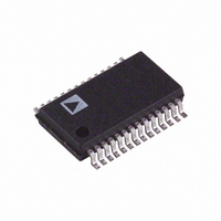
AD9201ARS Analog Devices Inc, AD9201ARS Datasheet - Page 5

AD9201ARS
Manufacturer Part Number
AD9201ARS
Description
IC ADC CMOS 10BIT DUAL 28-SSOP
Manufacturer
Analog Devices Inc
Specifications of AD9201ARS
Mounting Type
Surface Mount
Rohs Status
RoHS non-compliant
Number Of Bits
10
Sampling Rate (per Second)
20M
Data Interface
Parallel
Number Of Converters
2
Power Dissipation (max)
245mW
Voltage Supply Source
Analog and Digital
Operating Temperature
-40°C ~ 85°C
Package / Case
28-SSOP (0.200", 5.30mm Width)
Input Channels Per Adc
2
No. Of Channels
2
Peak Reflow Compatible (260 C)
No
Inl ±
2.5LSB
Sample Rate
20MSPS
No. Of Bits
10 Bit
Leaded Process Compatible
No
Dnl±
1LSB
Number Of Elements
2
Resolution
10Bit
Architecture
Pipelined
Input Polarity
Unipolar
Input Type
Voltage
Rated Input Volt
1.5V
Differential Input
Yes
Power Supply Requirement
Analog and Digital
Single Supply Voltage (typ)
3V
Single Supply Voltage (min)
2.7V
Single Supply Voltage (max)
5.5V
Dual Supply Voltage (typ)
Not RequiredV
Dual Supply Voltage (min)
Not RequiredV
Dual Supply Voltage (max)
Not RequiredV
Differential Linearity Error
±1LSB
Integral Nonlinearity Error
±2.5LSB
Operating Temp Range
-40C to 85C
Operating Temperature Classification
Industrial
Mounting
Surface Mount
Pin Count
28
Package Type
SSOP
Lead Free Status / Rohs Status
Not Compliant
Available stocks
Company
Part Number
Manufacturer
Quantity
Price
Part Number:
AD9201ARS
Manufacturer:
ADI/亚德诺
Quantity:
20 000
Part Number:
AD9201ARSZ
Manufacturer:
ADI/亚德诺
Quantity:
20 000
Company:
Part Number:
AD9201ARSZ-REEL
Manufacturer:
SIEMENS
Quantity:
3
OFFSET ERROR
The first transition should occur at a level 1 LSB above “zero.”
Offset is defined as the deviation of the actual first code transi-
tion from that point.
OFFSET MATCH
The change in offset error between I and Q channels.
EFFECTIVE NUMBER OF BITS (ENOB)
For a sine wave, SINAD can be expressed in terms of the num-
ber of bits. Using the following formula,
It is possible to get a measure of performance expressed as N,
the effective number of bits.
Thus, effective number of bits for a device for sine wave inputs
at a given input frequency can be calculated directly from its
measured SINAD.
TOTAL HARMONIC DISTORTION (THD)
THD is the ratio of the rms sum of the first six harmonic com-
ponents to the rms value of the measured input signal and
is expressed as a percentage or in decibels.
SIGNAL-TO-NOISE RATIO (SNR)
SNR is the ratio of the rms value of the measured input signal to
the rms sum of all other spectral components below the Nyquist
frequency, excluding the first six harmonics and dc. The value
for SNR is expressed in decibels.
SPURIOUS FREE DYNAMIC RANGE (SFDR)
The difference in dB between the rms amplitude of the input
signal and the peak spurious signal.
GAIN ERROR
The first code transition should occur for an analog value 1 LSB
above nominal negative full scale. The last transition should
occur for an analog value 1 LSB below the nominal positive full
REV. D
AVSS
N = (SINAD – 1.76)/6.02
IN
d. INA, INB
a. D0–D9, OTR
AVDD
AVDD
AVSS
AVDD
AVSS
DRVSS
DRVDD
DRVSS
REFBS
REFBF
AVDD
e. Reference
Figure 2. Equivalent Circuits
AVDD
AVSS
AVSS
b. Three-State, Standby
AVSS
AVDD
–5–
scale. Gain error is the deviation of the actual difference be-
tween first and last code transitions and the ideal difference
between the first and last code transitions.
GAIN MATCH
The change in gain error between I and Q channels.
PIPELINE DELAY (LATENCY)
The number of clock cycles between conversion initiation and
the associated output data being made available. New output
data is provided every rising clock edge.
MUX SELECT DELAY
The delay between the change in SELECT pin data level and
valid data on output pins.
POWER SUPPLY REJECTION
The specification shows the maximum change in full scale from
the value with the supply at the minimum limit to the value with
the supply at its maximum limit.
APERTURE JITTER
Aperture jitter is the variation in aperture delay for successive
samples and is manifested as noise on the input to the A/D.
APERTURE DELAY
Aperture delay is a measure of the Sample-and-Hold Amplifier
(SHA) performance and is measured from the rising edge of the
clock input to when the input signal is held for conversion.
SIGNAL-TO-NOISE AND DISTORTION (S/N+D, SINAD)
RATIO
S/N+D is the ratio of the rms value of the measured input signal
to the rms sum of all other spectral components below the
Nyquist frequency, including harmonics but excluding dc.
The value for S/N+D is expressed in decibels.
AVSS
AVDD
f. REFSENSE
AVDD
AVSS
AVSS
AVDD
g. VREF
AVDD
AVSS
c. CLK
AVSS
AVDD
AD9201


