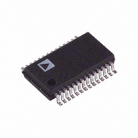
AD9201ARS Analog Devices Inc, AD9201ARS Datasheet - Page 9

AD9201ARS
Manufacturer Part Number
AD9201ARS
Description
IC ADC CMOS 10BIT DUAL 28-SSOP
Manufacturer
Analog Devices Inc
Specifications of AD9201ARS
Mounting Type
Surface Mount
Rohs Status
RoHS non-compliant
Number Of Bits
10
Sampling Rate (per Second)
20M
Data Interface
Parallel
Number Of Converters
2
Power Dissipation (max)
245mW
Voltage Supply Source
Analog and Digital
Operating Temperature
-40°C ~ 85°C
Package / Case
28-SSOP (0.200", 5.30mm Width)
Input Channels Per Adc
2
No. Of Channels
2
Peak Reflow Compatible (260 C)
No
Inl ±
2.5LSB
Sample Rate
20MSPS
No. Of Bits
10 Bit
Leaded Process Compatible
No
Dnl±
1LSB
Number Of Elements
2
Resolution
10Bit
Architecture
Pipelined
Input Polarity
Unipolar
Input Type
Voltage
Rated Input Volt
1.5V
Differential Input
Yes
Power Supply Requirement
Analog and Digital
Single Supply Voltage (typ)
3V
Single Supply Voltage (min)
2.7V
Single Supply Voltage (max)
5.5V
Dual Supply Voltage (typ)
Not RequiredV
Dual Supply Voltage (min)
Not RequiredV
Dual Supply Voltage (max)
Not RequiredV
Differential Linearity Error
±1LSB
Integral Nonlinearity Error
±2.5LSB
Operating Temp Range
-40C to 85C
Operating Temperature Classification
Industrial
Mounting
Surface Mount
Pin Count
28
Package Type
SSOP
Lead Free Status / Rohs Status
Not Compliant
Available stocks
Company
Part Number
Manufacturer
Quantity
Price
Part Number:
AD9201ARS
Manufacturer:
ADI/亚德诺
Quantity:
20 000
Part Number:
AD9201ARSZ
Manufacturer:
ADI/亚德诺
Quantity:
20 000
Company:
Part Number:
AD9201ARSZ-REEL
Manufacturer:
SIEMENS
Quantity:
3
The AD9201 can accommodate a variety of input spans be-
tween 1 V and 2 V. For spans of less than 1 V, expect a propor-
tionate degradation in SNR . Use of a 2 V span will provide the
best noise performance. 1 V spans will provide lower distortion
when using a 3 V analog supply. Users wishing to run with
larger full-scales are encouraged to use a 5 V analog supply
(AVDD).
Single-Ended Inputs: For single-ended input signals, the
signal is applied to one input pin and the other input pin is tied
to a midscale voltage. This midscale voltage defines the center
of the full-scale span for the input signal.
EXAMPLE: For a single-ended input range from 0 V to 1 V
applied to IINA, we would configure the converter for a 1 V
reference (See Figure 17) and apply 0.5 V to IINB.
Note that since the inputs are high impedance, this reference
level can easily be generated with an external resistive divider
with large resistance values (to minimize power dissipation). A
decoupling capacitor is recommended on this input to minimize
the high frequency noise-coupling onto this pin. Decoupling
should occur close to the ADC.
Differential Inputs
Use of differential input signals can provide greater flexibility in
input ranges and bias points, as well as offering improvements in
distortion performance, particularly for high frequency input
signals. Users with differential input signals will probably want
to take advantage of the differential input structure.
REV. D
Figure 18. Example Configuration for 0.5 V–1.5 V ac
Coupled Single-Ended Inputs
MIDSCALE
ANALOG
VOLTAGE
Figure 17. Example Configuration for 0 V–1 V Single-
Ended Input Signal
INPUT
INPUT
= 0.5V
5k
1.0 F
1V
0V
C2
C1
10 F
1.5V
0.5V
5k
0.1 F
R1
1k
C3
0.1 F
0.1 F
VREF
REFSENSE
IINA
IINB
IINA
IINB
VREF
REFSENSE
AD9201
AD9201
10 F
I OR QREFB
I OR QREFT
REFB
REFT
0.1 F
0.1 F
10 F
0.1 F
10 F
0.1 F
0.1 F
0.1 F
–9–
AC Coupled Inputs
If the signal of interest has no dc component, ac coupling can be
easily used to define an optimum bias point. Figure 18 illus-
trates one recommended configuration. The voltage chosen for
the dc bias point (in this case the 1 V reference) is applied to
both IINA and IINB pins through 1 k resistors (R1 and R2).
IINA is coupled to the input signal through Capacitor C1, while
IINB is decoupled to ground through Capacitor C2 and C3.
Transformer Coupled Inputs
Another option for input ac coupling is to use a transformer.
This not only provides dc rejection, but also allows truly differ-
ential drive of the AD9201’s analog inputs, which will provide
the optimal distortion performance. Figure 19 shows a recom-
mended transformer input drive configuration. Resistors R1 and
R2 define the termination impedance of the transformer coupling.
The center tap of the transformer secondary is tied to the com-
mon-mode reference, establishing the dc bias point for the ana-
log inputs.
Crosstalk: The internal layout of the AD9201, as well as its
pinout, was configured to minimize the crosstalk between the
two input signals. Users wishing to minimize high frequency
crosstalk should take care to provide the best possible decoupling
for input pins (see Figure 20). R and C values will make a pole
dependant on antialiasing requirements. Decoupling is also
required on reference pins and power supplies (see Figure 21).
Figure 19. Example Configuration for Transformer
Coupled Inputs
Figure 21. Reference and Power Supply Decoupling
V ANALOG
VOLTAGE
COMMON
10 F
10 F
MODE
0.1 F
Figure 20. Input Loading
0.1 F
R1
IINA
IINB
AVDD
IINA
IINB
VREF
AD9201
REFSENSE
AD9201
I OR QREFB
I OR QREFT
AD9201
I OR QREFB
I OR QREFT
DVDD
QINA
QINB
QINA
QINB
0.1 F
0.1 F
R2
0.1 F
AD9201
V DIGITAL
10 F
10 F
0.1 F
10 F
0.1 F
0.1 F
0.1 F


