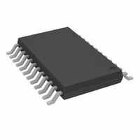
AD7794BRUZ Analog Devices Inc, AD7794BRUZ Datasheet - Page 17

AD7794BRUZ
Manufacturer Part Number
AD7794BRUZ
Description
IC ADC 24BIT SIG-DEL 6CH 24TSSOP
Manufacturer
Analog Devices Inc
Datasheet
1.AD7795BRUZ.pdf
(36 pages)
Specifications of AD7794BRUZ
Data Interface
DSP, MICROWIRE™, QSPI™, Serial, SPI™
Number Of Bits
24
Sampling Rate (per Second)
470
Number Of Converters
1
Power Dissipation (max)
2.5mW
Voltage Supply Source
Analog and Digital
Operating Temperature
-40°C ~ 105°C
Mounting Type
Surface Mount
Package / Case
24-TSSOP (0.173", 4.40mm Width)
Resolution (bits)
24bit
Sampling Rate
470SPS
Input Channel Type
Differential
Supply Voltage Range - Analog
2.7V To 5.25V
Supply Voltage Range - Digital
2.7V To 5.25V
Number Of Elements
1
Resolution
24Bit
Architecture
Delta-Sigma
Sample Rate
0.47KSPS
Input Polarity
Bipolar
Input Type
Voltage
Rated Input Volt
±2.5V
Differential Input
Yes
Power Supply Requirement
Single
Single Supply Voltage (typ)
3.3/5V
Single Supply Voltage (min)
2.7V
Single Supply Voltage (max)
5.25V
Dual Supply Voltage (typ)
Not RequiredV
Dual Supply Voltage (min)
Not RequiredV
Dual Supply Voltage (max)
Not RequiredV
Power Dissipation
2.5mW
Integral Nonlinearity Error
±15ppm of FSR
Operating Temp Range
-40C to 105C
Operating Temperature Classification
Industrial
Mounting
Surface Mount
Pin Count
24
Package Type
TSSOP
Input Signal Type
Differential
Lead Free Status / RoHS Status
Lead free / RoHS Compliant
For Use With
EVAL-AD7794EBZ - BOARD EVALUATION FOR AD7794
Lead Free Status / Rohs Status
Compliant
Available stocks
Company
Part Number
Manufacturer
Quantity
Price
Company:
Part Number:
AD7794BRUZ
Manufacturer:
ADI
Quantity:
2 429
Part Number:
AD7794BRUZ
Manufacturer:
AD
Quantity:
20 000
Part Number:
AD7794BRUZ-REEL
Manufacturer:
ADI/亚德诺
Quantity:
20 000
ON-CHIP REGISTERS
The ADC is controlled and configured via a number of on-chip
registers that are described in the following sections. In the
following descriptions, set implies a Logic 1 state and cleared
implies a Logic 0 state, unless otherwise noted.
COMMUNICATIONS REGISTER
RS2, RS1, RS0 = 0, 0, 0
The communications register is an 8-bit write-only register. All
communications to the part must start with a write operation to
the communications register. The data written to the communi-
cations register determines whether the next operation is a read
or write operation, and to which register this operation takes
place. For read or write operations, once the subsequent read or
write operation to the selected register is complete, the interface
CR7
WEN(0)
Table 14. Communications Register Bit Designations
Bit No.
CR7
CR6
CR5 to
CR3
CR2
CR1 to
CR0
Table 15. Register Selection
RS2
0
0
0
0
0
1
1
1
1
RS1
0
0
0
1
1
0
0
1
1
Mnemonic
WEN
R/W
RS2 to RS0
CREAD
0
RS0
0
0
1
0
1
0
1
0
1
CR6
R/W(0)
Description
Write Enable Bit. A 0 must be written to this bit so that the write to the communications register actually occurs. If
a 1 is the first bit written, the part does not clock on to subsequent bits in the register. It stays at this bit location
until a 0 is written to this bit. Once a 0 is written to the WEN bit, the next seven bits are loaded to the
communications register.
A 0 in this bit location indicates that the next operation is a write to a specified register. A 1 in this position
indicates that the next operation is a read from the designated register.
Register Address Bits. These address bits are used to select which registers of the ADC are being selected during
this serial interface communication. See Table 15.
Continuous Read of the Data Register. When this bit is set to 1 (and the data register is selected), the serial
interface is configured so that the data register can be read continuously, that is, the contents of the data register
are automatically placed on the DOUT pin when the SCLK pulses are applied after the RDY pin goes low to
indicate that a conversion is complete. The communications register does not have to be written to for data reads.
To enable continuous read mode, the instruction 01011100 must be written to the communications register. To
exit the continuous read mode, the instruction 01011000 must be written to the communications register while
the RDY pin is low. While in continuous read mode, the ADC monitors activity on the DIN line so it can receive the
instruction to exit continuous read mode. Additionally, a reset occurs if 32 consecutive 1s are seen on DIN.
Therefore, DIN should be held low in continuous read mode until an instruction is written to the device.
These bits must be programmed to Logic 0 for correct operation.
Register
Communications Register During a Write Operation
Status Register During a Read Operation
Mode Register
Configuration Register
Data Register
ID Register
IO Register
Offset Register
Full-Scale Register
CR5
RS2(0)
CR4
RS1(0)
Rev. D | Page 17 of 36
CR3
RS0(0)
returns to where it expects a write operation to the
communications register. This is the default state of the
interface and, on power-up or after a reset, the ADC is in this
default state waiting for a write operation to the communications
register. In situations where the interface sequence is lost, a
write operation of at least 32 serial clock cycles with DIN high
returns the ADC to this default state by resetting the entire part.
Table 14 outlines the bit designations for the communications
register. CR0 through CR7 indicate the bit location, with CR
denoting the bits are in the communications register. CR7
denotes the first bit of the data stream. The number in brackets
indicates the power-on/reset default status of that bit.
CR2
CREAD(0)
Register Size
8-bit
8-bit
16-bit
16-bit
24-bit (AD7794)/16-Bit (AD7795)
8-bit
8-bit
24-bit (AD7794)/16-Bit (AD7795)
24-bit (AD7794)/16-Bit (AD7795)
AD7794/AD7795
CR1
0(0)
CR0
0(0)


