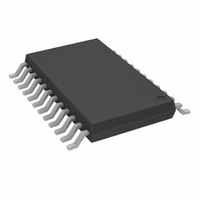
AD7794BRUZ Analog Devices Inc, AD7794BRUZ Datasheet - Page 19

AD7794BRUZ
Manufacturer Part Number
AD7794BRUZ
Description
IC ADC 24BIT SIG-DEL 6CH 24TSSOP
Manufacturer
Analog Devices Inc
Datasheet
1.AD7795BRUZ.pdf
(36 pages)
Specifications of AD7794BRUZ
Data Interface
DSP, MICROWIRE™, QSPI™, Serial, SPI™
Number Of Bits
24
Sampling Rate (per Second)
470
Number Of Converters
1
Power Dissipation (max)
2.5mW
Voltage Supply Source
Analog and Digital
Operating Temperature
-40°C ~ 105°C
Mounting Type
Surface Mount
Package / Case
24-TSSOP (0.173", 4.40mm Width)
Resolution (bits)
24bit
Sampling Rate
470SPS
Input Channel Type
Differential
Supply Voltage Range - Analog
2.7V To 5.25V
Supply Voltage Range - Digital
2.7V To 5.25V
Number Of Elements
1
Resolution
24Bit
Architecture
Delta-Sigma
Sample Rate
0.47KSPS
Input Polarity
Bipolar
Input Type
Voltage
Rated Input Volt
±2.5V
Differential Input
Yes
Power Supply Requirement
Single
Single Supply Voltage (typ)
3.3/5V
Single Supply Voltage (min)
2.7V
Single Supply Voltage (max)
5.25V
Dual Supply Voltage (typ)
Not RequiredV
Dual Supply Voltage (min)
Not RequiredV
Dual Supply Voltage (max)
Not RequiredV
Power Dissipation
2.5mW
Integral Nonlinearity Error
±15ppm of FSR
Operating Temp Range
-40C to 105C
Operating Temperature Classification
Industrial
Mounting
Surface Mount
Pin Count
24
Package Type
TSSOP
Input Signal Type
Differential
Lead Free Status / RoHS Status
Lead free / RoHS Compliant
For Use With
EVAL-AD7794EBZ - BOARD EVALUATION FOR AD7794
Lead Free Status / Rohs Status
Compliant
Available stocks
Company
Part Number
Manufacturer
Quantity
Price
Company:
Part Number:
AD7794BRUZ
Manufacturer:
ADI
Quantity:
2 429
Part Number:
AD7794BRUZ
Manufacturer:
AD
Quantity:
20 000
Part Number:
AD7794BRUZ-REEL
Manufacturer:
ADI/亚德诺
Quantity:
20 000
MODE REGISTER
RS2, RS1, RS0 = 0, 0, 1; Power-On/Reset = 0x000A
The mode register is a 16-bit read/write register that is used to
select the operating mode, the update rate, and the clock source.
Table 17 outlines the bit designations for the mode register.
MR0 through MR15 indicate the bit locations with MR
MR15
MD2(0)
MR7
CLK1(0)
Table 17. Mode Register Bit Designations
Bit No.
MR15 to MR13
MR12
MR11 to MR10
MR9
MR8
MR7 to MR6
MR5
MR4
MR3 to MR0
MR14
MD1(0)
MR6
CLK0(0)
Mnemonic
MD2 to MD0
PSW
0
AMP-CM
0
CLK1 to CLK0
0
CHOP-DIS
FS3 to FS0
MR13
MD0(0)
MR5
0(0)
Description
Mode Select Bits. These bits select the operating mode of the AD7794/AD7795 (see Table 18).
Power Switch Control Bit. Set by user to close the power switch PSW to GND. The power switch can sink
up to 30 mA. Cleared by user to open the power switch. When the ADC is placed in power-down mode,
the power switch is opened.
These bits must be programmed with a Logic 0 for correct operation.
Instrumentation Amplifier Common-Mode Bit. This bit is used in conjunction with the CHOP-DIS bit. With
chop disabled, the user can operate with a wider range of common-mode voltages when AMP-CM is
cleared. However, the dc common-mode rejection degrades. With AMP-CM set, the span for the common-
mode voltage is reduced (see the Specifications section). However, the dc common-mode rejection is
significantly better.
This bit must be programmed with a Logic 0 for correct operation.
These bits are used to select the clock source for the AD7794/AD7795. Either the on-chip 64 kHz clock can
be used or an external clock can be used. The ability to use an external clock allows several AD7794/AD7795
devices to be synchronized. Also, 50 Hz/60 Hz rejection is improved when an accurate external clock
drives the AD7794/AD7795.
CLK1
0
0
1
1
This bit must be programmed with a Logic 0 for correct operation.
This bit is used to enable or disable chop. On power-up or following a reset, CHOP-DIS is cleared so chop is
enabled. When CHOP-DIS is set, chop is disabled. This bit is used in conjunction with the AMP-CM bit.
When chop is disabled, the AMP-CM bit should be set. This limits the common-mode voltage that can be
used by the ADC, but the dc common-mode rejection does not degrade.
Filter Update Rate Select Bits (see Table 19).
CLK0
0
1
0
1
MR12
PSW(0)
MR4
CHOP-DIS(0)
ADC Clock Source
Internal 64 kHz clock. Internal clock is not available at the CLK pin.
Internal 64 kHz clock. This clock is made available at the CLK pin.
External 64 kHz. The external clock can have a 45:55 duty cycle (see the
Specifications section for the external clock).
External clock. The external clock is divided by 2 within the AD7794/AD7795.
Rev. D | Page 19 of 36
denoting that the bits are in the mode register. MR15 is the first
bit of the data stream. The number in parentheses indicates the
power-on/reset default status of that bit. Any write to the setup
register resets the modulator and filter, and sets the RDY bit.
MR11
MR3
0(0)
FS3(1)
MR10
0(0)
MR2
FS2(0)
MR9
AMP-CM(0)
MR1
FS1(1)
AD7794/AD7795
MR8
0(0)
MR0
FS0(0)


