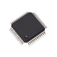
CS5366-CQZR Cirrus Logic Inc, CS5366-CQZR Datasheet - Page 19

CS5366-CQZR
Manufacturer Part Number
CS5366-CQZR
Description
IC ADC 6CH 114DB 216KHZ 48-LQFP
Manufacturer
Cirrus Logic Inc
Datasheet
1.CS5366-CQZ.pdf
(42 pages)
Specifications of CS5366-CQZR
Package / Case
48-LQFP
Number Of Bits
24
Sampling Rate (per Second)
216k
Data Interface
Serial
Number Of Converters
1
Power Dissipation (max)
830mW
Voltage Supply Source
Analog and Digital
Operating Temperature
-40°C ~ 85°C
Mounting Type
Surface Mount
Conversion Rate
192 KSPs
Resolution
24 bit
Number Of Adc Inputs
6
Operating Supply Voltage
5 V
Maximum Operating Temperature
+ 85 C
Minimum Operating Temperature
- 40 C
Mounting Style
SMD/SMT
Supply Voltage (max)
5.25 V
Supply Voltage (min)
4.75 V
Lead Free Status / RoHS Status
Lead free / RoHS Compliant
For Use With
598-1549 - BOARD EVAL FOR CS5366 192KHZ ADC
Lead Free Status / RoHS Status
Lead free / RoHS Compliant, Lead free / RoHS Compliant
Available stocks
Company
Part Number
Manufacturer
Quantity
Price
Company:
Part Number:
CS5366-CQZR
Manufacturer:
Cirrus Logic Inc
Quantity:
10 000
DS626F4
4. APPLICATIONS
4.1
4.2
4.2.1 Stand-Alone Mode
4.2.2 Control Port Mode
Power
CS5366 features five independent power pins that power various functional blocks within the device and
allow for convenient interfacing to other devices.
each supply pin. Please refer to
each power supply pin. The power supplied to each power pin can be independent of the power supplied to
any other pin.
To meet full performance specifications, the CS5366 requires normal low-noise board layout. The
Connection Diagram” on page 9
to a clean supply. VD, which powers the digital filter, may be run from the system logic supply, or it may be
powered from the analog supply via a single-pole decoupling filter.
Decoupling capacitors should be placed as near to the ADC as possible, with the lower value high-frequen-
cy capacitors placed nearest to the device leads. Clocks should be kept away from the FILT+ and VQ pins
in order to avoid unwanted coupling of these signals into the device. The FILT+ and VQ decoupling capac-
itors must be positioned to minimize the electrical path to ground.
The CDB5366 evaluation board demonstrates optimum layout for the device.
Control Port Mode and Stand-Alone Operation
In Stand-Alone Mode, the CS5366 is programmed exclusively with multi-use configuration pins. This mode
provides a set of commonly used features, which comprise a subset of the complete set of device features
offered in Control Port Mode.
To use the CS5366 in Stand-Alone Mode, the configuration pins must be held in a stable state, at valid logic
levels, and RST must be asserted until the power supplies and clocks are stable and valid. More informa-
tion on the reset function is available in
In Control Port Mode, all features of the CS5366 are available. Four multi-use configuration pins become
software pins that support the I²C or SPI bus protocol. To initiate Control Port Mode, a controller that sup-
ports I²C or SPI must be used to enable the internal register functionality. This is done by setting the CP-
EN bit (Bit 7 of the Global Control Port Register). Once CP-EN is set, all of the device configuration pins
are ignored, and the internal register settings determine the operating modes of the part.
page 30
provides detailed information about the I²C and SPI bus protocols.
Pin Name
VLS
VLC
VX
VD
VA
Power Supply Pin
Table 1. Power Supply Pin Definitions
shows the recommended power arrangements, with the VA pins connected
“Recommended Operating Conditions” on page 10
Pin Number
Section 4.5 on page
4, 9
20
33
28
35
Table 1
shows what portion of the device is powered from
Serial Audio Interface
Functional Block
Crystal Oscillator
22.
Control Logic
Analog Core
Digital Core
for the valid range of
Figure 4.13 on
CS5366
“Typical
19


