AD9237BCPZ-20 Analog Devices Inc, AD9237BCPZ-20 Datasheet
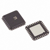
IC ADC 12BIT SGL 20MSPS 32LFCSP

AD9237BCPZ-20

Manufacturer Part Number
AD9237BCPZ-20
Description
IC ADC 12BIT SGL 20MSPS 32LFCSP
Manufacturer
Analog Devices Inc
Datasheets

Specifications of AD9237BCPZ-20

Data Interface
Parallel
Number Of Bits
12
Sampling Rate (per Second)
20M
Number Of Converters
3
Power Dissipation (max)
85mW
Voltage Supply Source
Single Supply
Operating Temperature
-40°C ~ 85°C
Mounting Type
Surface Mount
Package / Case
32-VFQFN, CSP Exposed Pad
Resolution (bits)
12bit
Input Channel Type
Differential
Supply Voltage Range - Analogue
2.7V To 3.6V
Supply Voltage Range - Digital
2.25V To 3.6V
Supply Current
30.5mA
Sampling Rate
20MSPS
Rohs Compliant
Yes
Lead Free Status / RoHS Status
Lead free / RoHS Compliant

Available stocks

Company
Part Number
Manufacturer
Quantity
Price
Part Number:
AD9237BCPZ-20
Manufacturer:
INFINEON
Quantity:
2 300
Part Number:
AD9237BCPZ-20
Manufacturer:
ADI/亚德诺
Quantity:
20 000
a
Preliminary Technical Data
Ultra Low Power
SNR = 66.5 dBc (to Nyquist);
SFDR = 82 dBc @ 2.4MHz Analog Input
ENOB = 10.5 bits
DNL=± 0.5 LSB
Differential Input with 500MHz Full Power Bandwidth
Flexible and Selectable Analog Input: 4Vp-p to 1Vp-p
Data Formats Supported; Offset Binary, Twos
Complement and Gray Code
Output Enable Pin
2-step power down; Full Power down and Sleep mode
APPLICATIONS
Ultrasound and Medical Imaging
Battery Powered Instruments; Hand-Held
Scopemeters; Low Cost Digital Oscilloscopes; Low
Power Digital Still Cameras and Copiers; Low power
communications
PRODUCT DESCRIPTION
The AD9237 is a monolithic, single 3V supply, 12-bit,
20/40/65MSPS Analog to Digital Converter with a high
performance sample-and-hold amplifier and voltage
reference. The AD9237 uses a multistage differential
pipelined architecture with output error correction logic to
provide 12-bit accuracy at 20/40/65MSPS data rates and
guarantee no missing codes over the full operating
temperature range.
The wide bandwidth, truly differential SHA allows for a
variety of user-selectable input ranges and offsets including
single-ended applications. It is suitable for multiplexed
systems that switch full-scale voltage levels in successive
channels and for sampling single-channel inputs at
frequencies well beyond the Nyquist rate. With significant
power savings over previously available analog to digital
converters, the AD9237 is suitable for applications imaging
and medical ultrasound.
A single-ended clock input is used to control all internal
conversion cycles. The digital output data is presented in
straight binary, twos complement, or gray code formats. An
out-of-range (OTR) signal indicates an overflow condition,
which can be used with the most significant bit to determine
low or high overflow.
REV PrF 5/18/2005
Information furnished by Analog Devices is believed to be accurate and reliable.
However, no responsibility is assumed by Analog Devices for its use, nor for any
infringements of patents or other rights of third parties that may result from its use.
No license is granted by implication or otherwise under any patent or patent rights
of Analog Devices.
FEATURES
135mW @ 40MSPS;
190mW @ 65MSPS
90mW @ 20MSPS;
SENSE
REFB
REFT
VREF
VINB
VINA
One Technology Way, P.O Box 9106, Norwood, MA 02062–9106, U.S.A.
Tel: 617/329–4700
Fax: 617–326–8703
3 V Low Power A/D Converter
Fabricated on an advanced CMOS process, the AD9237 is
available in a 32-pin chip scale package and is specified
over the industrial temperature range (-40°C to +85°C).
PRODUCT HIGHLIGHTS
1.
2.
3.
4.
5.
6.
7.
8.
AVDD
SHA
SELECT
Operating at 65MSPS, the AD9237 consumes a low
190mW and only consumes 135mW at 40 MSPS and
90mW at 20MSPS.
The AD9237 operates from a single 3V power supply,
and features a separate digital output driver supply to
accommodate 2.5V and 3.3V logic families.
The patented SHA input maintains excellent
performance for input frequencies beyond Nyquist, and
can be configured for single-ended or differential
operation.
The AD9237 is pin compatible to the AD9235, a 12-bit,
20/40/65 MSPS A/D converter. This allows a simplified
path for low power 12-bit systems.
The AD9237 is optimized for selectable and flexible
input ranges from 4Vp-p to 1Vp-p.
Output Enable pin to allow for multiplexing of the
outputs.
Two-step power down supports a standby mode in
addition to a power down mode.
The OTR output bit indicates when the signal is beyond
the selected input range.
REF
AD9237
A/D
FUNCTIONAL BLOCK DIAGRAM
AVSS
12-Bit, 20/40/65 MSPS
MDAC1
4
0.5 V
CLOCK
World Wide Web Site: http://www.analog.com
CORRECTION LOGIC
OUTPUT BUFFERS
PDWN
8-STAGE Pipeline
MODE2
16
12
AD9237
© Analog Devices, Inc., 2005
SELECT
MODE
MODE
DRVSS
A/D
DRVDD
3
OE
OTR
D11 (MSB)
D0 (LSB)

Related parts for AD9237BCPZ-20

AD9237BCPZ-20 Summary of contents

Page 1

Preliminary Technical Data FEATURES Ultra Low Power 90mW @ 20MSPS; 135mW @ 40MSPS; 190mW @ 65MSPS SNR = 66.5 dBc (to Nyquist); SFDR = 82 dBc @ 2.4MHz Analog Input ENOB = 10.5 bits DNL=± 0.5 LSB Differential Input ...

Page 2

... Power Down Mode power is measured with a dc input, the CLK pin inactive (i.e., set to AVDD or AGND) 6. Standby Mode power is measured with a dc input, the CLK pin active. Specifications subject to change without notice. AD9237 Preliminary Technical Information – 5/18/2005 Preliminary Technical Data AD9237BCPZ-20 Test Temp Level Min Typ ...

Page 3

... Full V 2 Full IV 3.29 Full IV 3.25 Full IV 0.2 Full IV 0.05 Full IV 2.49 Full IV 2.45 Full IV 0.2 Full IV 0.05 AD9237BCPZ-20 Test Temp Level Min Typ Max Full IV 20 Full V 1 Full V 50.0 Full V 15 Full V 15 Full V 3.5 Full V 9 Full ...

Page 4

... MHz INPUT F = 10.3 MHz INPUT F = 19.6 MHz INPUT MHz INPUT MHz INPUT Specifications subject to change without notice. AD9237 Preliminary Technical Information – 5/18/2005 Preliminary Technical Data AD9237BCPZ-20 Test Temp Level Min Typ Max Full IV 66.5 25°C I 66.5 Full IV 66.5 I 66.5 25° ...

Page 5

... JA JC ORDERING GUIDE Package Description 32-Lead Frame Chip Scale Package (LFCSP) 32-Lead Frame Chip Scale Package (LFCSP) 32-Lead Frame Chip Scale Package (LFCSP) LFCSP Evaluation Board (w/ AD9237BCPZ-20) LFCSP Evaluation Board (w/ AD9237BCPZ-40) LFCSP Evaluation Board (w/ AD9237BCPZ-65) –5– AD9237 Package Option CP-32 ...

Page 6

AD9237 DEFINITIONS OF SPECIFICATIONS INTEGRAL NONLINEARITY (INL) INL refers to the deviation of each individual code from a line drawn from “negative full scale” through “positive full scale.” The point used as “negative full scale” occurs 1/2 LSB before the ...

Page 7

Preliminary Technical Data PIN FUNCTION DESCRIPTIONS (32 Pin LFCSP Package) Pin No. Name 1 MODE 2 2 CLK PDWN 5,6 DNC 7-14, 17-20 D0 (LSB) – D11 (MSB) 15 DGND 16 DRVDD 21 OTR 22 MODE 23 ...

Page 8

AD9237 TYPICAL PERFORMANCE CHARACTERISTICS (AVDD = 3.0 V, DRVDD = 3 SAMPLE 25°C, unless otherwise noted Figure 2. AD9237-65 Analog Current vs. Clock Frequency vs. Power ...

Page 9

Preliminary Technical Data AD9237 Preliminary Technical Information – 5/18/2005 32-LFCSP Package Dimensions –9– AD9237 REV PrF ...

Related keywords