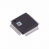
AD7661ASTZ Analog Devices Inc, AD7661ASTZ Datasheet - Page 20

AD7661ASTZ
Manufacturer Part Number
AD7661ASTZ
Description
IC ADC 16BIT W/REF 48-LQFP
Manufacturer
Analog Devices Inc
Series
PulSAR®r
Datasheet
1.AD7661ACPZRL.pdf
(28 pages)
Specifications of AD7661ASTZ
Data Interface
Serial, Parallel
Number Of Bits
16
Sampling Rate (per Second)
100k
Number Of Converters
1
Power Dissipation (max)
25mW
Voltage Supply Source
Analog and Digital
Operating Temperature
-40°C ~ 85°C
Mounting Type
Surface Mount
Package / Case
48-LQFP
Resolution (bits)
16bit
Input Channel Type
Pseudo Differential
Supply Voltage Range - Analogue
4.75V To 5.25V
Supply Voltage Range - Digital
2.7V To 5.25V,
Sampling Rate
100kSPS
Rohs Compliant
Yes
Number Of Elements
1
Resolution
16Bit
Architecture
SAR
Sample Rate
100KSPS
Input Polarity
Unipolar
Input Type
Voltage
Rated Input Volt
2.5V
Differential Input
Yes
Power Supply Requirement
Analog and Digital
Single Supply Voltage (typ)
5V
Single Supply Voltage (min)
4.75V
Single Supply Voltage (max)
5.25V
Dual Supply Voltage (typ)
Not RequiredV
Dual Supply Voltage (min)
Not RequiredV
Dual Supply Voltage (max)
Not RequiredV
Power Dissipation
45mW
Differential Linearity Error
-1LSB/1.5LSB
Integral Nonlinearity Error
±2.5LSB
Operating Temp Range
-40C to 85C
Operating Temperature Classification
Industrial
Mounting
Surface Mount
Pin Count
48
Package Type
LQFP
Input Signal Type
Pseudo-Differential
Lead Free Status / RoHS Status
Lead free / RoHS Compliant
For Use With
EVAL-AD7661CBZ - BOARD EVALUATION FOR AD7661
Lead Free Status / Rohs Status
Compliant
Available stocks
Company
Part Number
Manufacturer
Quantity
Price
Company:
Part Number:
AD7661ASTZ
Manufacturer:
ADI
Quantity:
390
Company:
Part Number:
AD7661ASTZ
Manufacturer:
Analog Devices Inc
Quantity:
10 000
Part Number:
AD7661ASTZ
Manufacturer:
ADI/亚德诺
Quantity:
20 000
Company:
Part Number:
AD7661ASTZRL
Manufacturer:
Analog Devices Inc
Quantity:
10 000
AD7661
For applications that use multiple AD7661s, it is more effective
to use the internal buffer to buffer the reference voltage.
Care should be taken with the voltage reference’s temperature
coefficient, which directly affects the full-scale accuracy if this
parameter matters. For instance, a ±15 ppm/°C temperature
coefficient of the reference changes full scale by ±1 LSB/°C.
Note that V
input range is defined in terms of V
increase the range to 0 V to 3 V with an AVDD above 4.85 V.
The
The TEMP pin, which measures the temperature of the
AD7661, can be used as shown in Figure 30. The output of
TEMP pin is applied to one of the inputs of the analog switch
(e.g., ADG779), and the ADC itself is used to measure its own
temperature. This configuration is very useful for improving the
calibration accuracy over the temperature range.
Power Supply
The AD7661 uses three power supply pins: an analog 5 V supply
AVDD, a digital 5 V core supply DVDD, and a digital input/
output interface supply OVDD. OVDD allows direct interface
with any logic between 2.7 V and DVDD + 0.3 V. To reduce the
supplies needed, the digital core (DVDD) can be supplied
through a simple RC filter from the analog supply, as shown in
Figure 26. The AD7661 is independent of power supply
sequencing once OVDD does not exceed DVDD by more than
0.3 V, and is thus free of supply voltage induced latch-up.
Additionally, it is very insensitive to power supply variations
over a wide frequency range, as shown in Figure 31, which
represents PSRR over frequency with on chip and external
references.
ANALOG INPUT
(UNIPOLAR)
AD780
Figure 30. Temperature Sensor Connection Diagram
REF
can be selected with a 3 V reference voltage.
ADG779
can be increased to AVDD – 1.85 V. Since the
AD8021
C
C
REF
IN
, this would essentially
TEMP
AD7661
TEMPERATURE
SENSOR
03033-0-024
Rev. 0 | Page 20 of 28
POWER DISSIPATION VERSUS THROUGHPUT
Operating currents are very low during the acquisition phase,
allowing significant power savings when the conversion rate is
reduced (see Figure 32). The AD7661 automatically reduces its
power consumption at the end of each conversion phase. This
makes the part ideal for very low power battery applications.
The digital interface and the reference remain active even
during the acquisition phase. To reduce operating digital supply
currents even further, digital inputs need to be driven close to
the power supply rails (i.e., DVDD or DGND), and OVDD
should not exceed DVDD by more than 0.3 V.
100000
10000
90
80
70
60
50
40
30
1000
100
10
1
10
Figure 32. Power Dissipation vs. Sampling Rate
Figure 31. PSRR vs. Frequency
INT REF
10
100
FREQUENCY (kHz)
SAMPLE RATE (SPS)
EXT REF
100
1000
PDREF = PDBUF = HIGH
1000
10000
10000
100000


