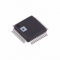
AD7661ASTZ Analog Devices Inc, AD7661ASTZ Datasheet - Page 24

AD7661ASTZ
Manufacturer Part Number
AD7661ASTZ
Description
IC ADC 16BIT W/REF 48-LQFP
Manufacturer
Analog Devices Inc
Series
PulSAR®r
Datasheet
1.AD7661ACPZRL.pdf
(28 pages)
Specifications of AD7661ASTZ
Data Interface
Serial, Parallel
Number Of Bits
16
Sampling Rate (per Second)
100k
Number Of Converters
1
Power Dissipation (max)
25mW
Voltage Supply Source
Analog and Digital
Operating Temperature
-40°C ~ 85°C
Mounting Type
Surface Mount
Package / Case
48-LQFP
Resolution (bits)
16bit
Input Channel Type
Pseudo Differential
Supply Voltage Range - Analogue
4.75V To 5.25V
Supply Voltage Range - Digital
2.7V To 5.25V,
Sampling Rate
100kSPS
Rohs Compliant
Yes
Number Of Elements
1
Resolution
16Bit
Architecture
SAR
Sample Rate
100KSPS
Input Polarity
Unipolar
Input Type
Voltage
Rated Input Volt
2.5V
Differential Input
Yes
Power Supply Requirement
Analog and Digital
Single Supply Voltage (typ)
5V
Single Supply Voltage (min)
4.75V
Single Supply Voltage (max)
5.25V
Dual Supply Voltage (typ)
Not RequiredV
Dual Supply Voltage (min)
Not RequiredV
Dual Supply Voltage (max)
Not RequiredV
Power Dissipation
45mW
Differential Linearity Error
-1LSB/1.5LSB
Integral Nonlinearity Error
±2.5LSB
Operating Temp Range
-40C to 85C
Operating Temperature Classification
Industrial
Mounting
Surface Mount
Pin Count
48
Package Type
LQFP
Input Signal Type
Pseudo-Differential
Lead Free Status / RoHS Status
Lead free / RoHS Compliant
For Use With
EVAL-AD7661CBZ - BOARD EVALUATION FOR AD7661
Lead Free Status / Rohs Status
Compliant
Available stocks
Company
Part Number
Manufacturer
Quantity
Price
Company:
Part Number:
AD7661ASTZ
Manufacturer:
ADI
Quantity:
390
Company:
Part Number:
AD7661ASTZ
Manufacturer:
Analog Devices Inc
Quantity:
10 000
Part Number:
AD7661ASTZ
Manufacturer:
ADI/亚德诺
Quantity:
20 000
Company:
Part Number:
AD7661ASTZRL
Manufacturer:
Analog Devices Inc
Quantity:
10 000
AD7661
SLAVE SERIAL INTERFACE
External Clock
The AD7661 is configured to accept an externally supplied
serial data clock on the SCLK pin when the EXT/ INT pin is
held HIGH. In this mode, several methods can be used to read
the data. The external serial clock is gated by CS . When CS and
RD are both LOW, the data can be read after each conversion or
during the following conversion. The external clock can be
either a continuous or a discontinuous clock. A discontinuous
clock can be either normally HIGH or normally LOW when
inactive. Figure 41 and Figure 42 show the detailed timing
diagrams of these methods. Usually, because the AD7661 has a
longer acquisition phase than conversion phase, the data are
read immediately after conversion.
SDOUT
CNVST
SDOUT
BUSY
SCLK
BUSY
SCLK
SDIN
CS
RD
t
16
Figure 42. Slave Serial Data Timing for Reading (Read Previous Conversion during Convert)
t
t
t
31
16
3
t
t
31
33
X
X
t
Figure 41. Slave Serial Data Timing for Reading (Read after Convert)
36
t
1
36
1
t
35
t
D15
t
35
37
D15
t
X15
37
t
34
2
2
EXT/INT = 1
D14
t
D14
X14
EXT/INT = 1
32
t
32
3
3
Rev. 0 | Page 24 of 28
D13
X13
D13
INVSCLK = 0
While the AD7661 is performing a bit decision, it is important
that voltage transients be avoided on digital input/output pins
or degradation of the conversion result could occur. This is
particularly important during the second half of the conversion
phase because the AD7661 provides error correction circuitry
that can correct for an improper bit decision made during the
first half of the conversion phase. For this reason, it is
recommended that when an external clock is being provided, it
is a discontinuous clock that is toggling only when BUSY is
LOW, or, more importantly, that it does not transition during
the latter half of BUSY HIGH.
INVSCLK = 0
14
14
15
15
D1
X1
D1
RD = 0
16
16
RD = 0
D0
X0
D0
17
X15
Y15
18
X14
Y14


