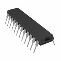
AD7731BNZ Analog Devices Inc, AD7731BNZ Datasheet - Page 35

AD7731BNZ
Manufacturer Part Number
AD7731BNZ
Description
IC ADC 24BIT SIGMA-DELTA 24DIP
Manufacturer
Analog Devices Inc
Datasheet
1.AD7731BRUZ.pdf
(44 pages)
Specifications of AD7731BNZ
Data Interface
DSP, Serial, SPI™
Number Of Bits
24
Sampling Rate (per Second)
6.4k
Number Of Converters
1
Power Dissipation (max)
125mW
Voltage Supply Source
Analog and Digital
Operating Temperature
-40°C ~ 85°C
Mounting Type
Through Hole
Package / Case
24-DIP (0.300", 7.62mm)
Resolution (bits)
24bit
Sampling Rate
6.4kSPS
Input Channel Type
Single Ended
Supply Voltage Range - Analog
4.75V To 5.25V
Supply Voltage Range - Digital
2.7V To 5.25V
Lead Free Status / RoHS Status
Lead free / RoHS Compliant
For Use With
EVAL-AD7731EBZ - BOARD EVALUATION FOR AD7731
Lead Free Status / RoHS Status
Lead free / RoHS Compliant, Lead free / RoHS Compliant
Read Operation
The reading of data from the part is from an output shift regis-
ter. On initiation of a read operation, data is transferred from
the specified register to the output shift register. This is a paral-
lel shift and is transparent to the user. Figure 16 shows a timing
diagram for a read operation from the output shift register of the
AD7731. With the POL input at a logic high, the data is clocked
out of the output shift register on the falling edge of SCLK.
With the POL input at a logic low, the data is clocked out of the
output shift register on the rising edge of SCLK.
Figure 16 also shows the CS input being used to decode the
read operation to the AD7731. However, this CS input can be
used in a number of different ways. It is possible to operate the
part in three-wire mode where the CS input is tied low perma-
nently. In this case, the SCLK line should idle high between
data transfer when the POL input is high and should idle low
between data transfers when the POL input is low. For POL = 1,
the first falling edge of SCLK clocks data from the output shift
register onto the DOUT line of the AD7731. It is then clocked
into the microcontroller on the next rising edge of SCLK. For
POL = 0, the first clock edge which clocks data from the AD7731
onto the DOUT line is a rising edge. It is then clocked into the
microcontroller on the next falling edge of SCLK.
In other microcontroller applications, which require a decoding
of the AD7731, CS can be generated from a port line. In this
case, CS would go low well in advance of the first falling edge of
SCLK (POL = 1) or the first rising edge of SCLK (POL = 0).
Clocking of each bit of data is as just described.
In DSP applications, the SCLK is generally a continuous clock.
In these applications, the CS input for the AD7731 is generated
from a frame synchronization signal from the DSP. In these
applications, the first edge after CS goes low is the active edge.
The MSB of the data to be shifted into the microcontroller must
REV. A
REV. 0
(POL = 0)
(POL = 1)
DOUT
SCLK
SCLK
RDY
CS
t
t
4
5A
t
3
Figure 17. Read Cycle Timing Diagram
MSB
t
5
t
6
t
7
–35–
be set up prior to this first active edge. Unlike microcontroller
applications, the DSP does not provide a clock edge to clock the
MSB from the AD7731. In this case, the CS of the AD7731
places the MSB on the DOUT line. For processors with the
rising edge of SCLK as the active edge, the POL input should
be tied high. In this case, the microcontroller takes data on the
rising edge. If CS goes low while SCLK is low, the MSB is
clocked out on the DOUT line from the CS. Subsequent data
bits are clocked from the falling edge of SCLK. For processors
with the falling edge of SCLK as the active edge, the POL input
should be tied low. In this case, the microcontroller takes data
on the falling edge. If CS goes low while SCLK is high, then the
MSB is clocked out on the DOUT line from the CS. Subse-
quent data bits are clocked from the rising edge of SCLK.
The RDY line is used as a status signal to indicate when data is
ready to be read from the AD7731’s data register. RDY goes
low when a new data word is available in the data register. It is
reset high when a read operation from the data register is com-
plete. It also goes high prior to the updating of the data register
to indicate when a read from the data register should not be
initiated. This is to ensure that the transfer of data from the data
register to the output shift register does not occur while the data
register is being updated. It is possible to read the same data
twice from the output register even though the RDY line returns
high after the first read operation. Care must be taken, however,
to ensure that the read operations are not initiated as the next
output update is about to take place.
For systems with a single data line, the DIN and DOUT lines
on the AD7731 can be connected together but care must be
taken in this case not to place the part in continuous read mode
as the part monitors DIN while supplying data on DOUT and
as a result, it may not be possible to take the part out of its
continuous read mode.
t
6
t
7
LSB
t
10
t
9
t
8
AD7731


