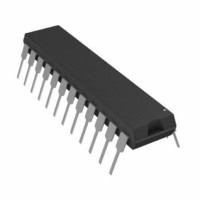
AD7731BNZ Analog Devices Inc, AD7731BNZ Datasheet - Page 37

AD7731BNZ
Manufacturer Part Number
AD7731BNZ
Description
IC ADC 24BIT SIGMA-DELTA 24DIP
Manufacturer
Analog Devices Inc
Datasheet
1.AD7731BRUZ.pdf
(44 pages)
Specifications of AD7731BNZ
Data Interface
DSP, Serial, SPI™
Number Of Bits
24
Sampling Rate (per Second)
6.4k
Number Of Converters
1
Power Dissipation (max)
125mW
Voltage Supply Source
Analog and Digital
Operating Temperature
-40°C ~ 85°C
Mounting Type
Through Hole
Package / Case
24-DIP (0.300", 7.62mm)
Resolution (bits)
24bit
Sampling Rate
6.4kSPS
Input Channel Type
Single Ended
Supply Voltage Range - Analog
4.75V To 5.25V
Supply Voltage Range - Digital
2.7V To 5.25V
Lead Free Status / RoHS Status
Lead free / RoHS Compliant
For Use With
EVAL-AD7731EBZ - BOARD EVALUATION FOR AD7731
Lead Free Status / RoHS Status
Lead free / RoHS Compliant, Lead free / RoHS Compliant
REV. A
MICROCOMPUTER/MICROPROCESSOR INTERFACING
The AD7731’s flexible serial interface allows for easy interface
to most microcomputers and microprocessors. The pseudo-code
of Table XVIII and Table XIX outline typical sequences for
interfacing a microcontroller or microprocessor to the AD7731.
Figures 18, 19 and 20 show some typical interface circuits.
The serial interface on the AD7731 has the capability of operat-
ing from just three wires and is compatible with SPI interface
protocols. The three-wire operation makes the part ideal for
isolated systems where minimizing the number of interface lines
minimizes the number of opto-isolators required in the system.
Register lengths on the AD7731 vary from 8 to 16 to 24 bits.
The 8-bit serial serial ports of most microcontrollers can handle
communication with these registers as either one, two or three
8-bit transfers. DSP processors and microprocessors generally
transfer 16 bits of data in a serial data operation. Some of these
processors, such as the ADSP-2105, have the facility to program
the amount of cycles in a serial transfer. This allows the user to
tailor the number of bits in any transfer to match the register
length of the required register in the AD7731. In any case,
writing 32 bits of data to a 24-bit register is not an issue pro-
vided the final 8 bits of the word are all 1s. This is because the
part returns to the Communications Register following a write
operation.
AD7731 to 68HC11 Interface
Figure 18 shows an interface between the AD7731 and the
68HC11 microcontroller. The diagram shows the minimum
(three-wire) interface with CS on the AD7731 hard-wired low.
In this scheme, the RDY bit of the Status Register is monitored
to determine when the Data Register is updated. An alternative
scheme, which increases the number of interface lines to four, is
to monitor the RDY output line from the AD7731. The moni-
toring of the RDY line can be done in two ways. First, RDY can
be connected to one of the 68HC11’s port bits (such as PC0)
which is configured as an input. This port bit is then polled to
determine the status of RDY. The second scheme is to use an
interrupt driven system in which case, the RDY output is con-
nected to the IRQ input of the 68HC11. For interfaces which
require control of the CS input on the AD7731, one of the port
bits of the 68HC11 (such as PC1), which is configured as an
output, can be used to drive the CS input.
The 68HC11 is configured in the master mode with its CPOL
bit set to a logic zero and its CPHA bit set to a logic one. When
the 68HC11 is configured like this, its SCLK line idles low
between data transfers. Therefore, the POL input of the AD7731
should be hard-wired low. For systems where it is preferable
REV. 0
–37–
that the SCLK idle high, the CPOL bit of the 68HC11 should
be set to a logic 1 and the POL input of the AD7731 should be
hard-wired to a logic high.
The AD7731 is not capable of full duplex operation. If the
AD7731 is configured for a write operation, no data appears on
the DATA OUT lines even when the SCLK input is active.
However, when the AD7731 is configured for continuous read
operation, data presented to the part on the DATA IN line is
monitored to determine when to exit the continuous read mode.
AD7731 to 8051 Interface
An interface circuit between the AD7731 and the 8XC51 micro-
controller is shown in Figure 19. The diagram shows the mini-
mum number of interface connections with CS on the AD7731
hard-wired low. In the case of the 8XC51 interface the mini-
mum number of interconnects is just two. In this scheme, the
RDY bit of the Status Register is monitored to determine when
the Data Register is updated. The alternative scheme, which
increases the number of interface lines to three, is to monitor
the RDY output line from the AD7731. The monitoring of the
RDY line can be done in two ways. First, RDY can be con-
nected to one of the 8XC51’s port bits (such as P1.0) which is
configured as an input. This port bit is then polled to determine
the status of RDY. The second scheme is to use an interrupt
driven system in which case, the RDY output is connected to
the INT1 input of the 8XC51. For interfaces which require
control of the CS input on the AD7731, one of the port bits of
the 8XC51 (such as P1.1), which is configured as an output,
can be used to drive the CS input.
Figure 18. AD7731 to 68HC11 Interface
68HC11
MISO
MOSI
SCK
SS
DV
DD
DV
DD
SYNC
RESET
SCLK
DATA OUT
DATA IN
CS
POL
AD7731
AD7731


