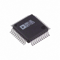
AD9260ASZ Analog Devices Inc, AD9260ASZ Datasheet - Page 33

AD9260ASZ
Manufacturer Part Number
AD9260ASZ
Description
IC ADC CMOS 16BIT OVRSAMP 44MQFP
Manufacturer
Analog Devices Inc
Datasheet
1.AD9260ASZRL.pdf
(44 pages)
Specifications of AD9260ASZ
Data Interface
Parallel
Number Of Bits
16
Sampling Rate (per Second)
20M
Number Of Converters
1
Power Dissipation (max)
585mW
Voltage Supply Source
Analog and Digital
Operating Temperature
-40°C ~ 85°C
Mounting Type
Surface Mount
Package / Case
44-MQFP, 44-PQFP
Resolution (bits)
16bit
Sampling Rate
2.5MSPS
Input Channel Type
Differential, Single Ended
Supply Voltage Range - Analog
4.75V To 5.25V
Number Of Elements
1
Resolution
16Bit
Architecture
Pipelined
Sample Rate
2.5MSPS
Input Polarity
Unipolar
Input Type
Voltage
Rated Input Volt
±0.8/±2V
Differential Input
Yes
Power Supply Requirement
Analog and Digital
Single Supply Voltage (typ)
5V
Single Supply Voltage (min)
4.75V
Single Supply Voltage (max)
5.25V
Dual Supply Voltage (typ)
Not RequiredV
Dual Supply Voltage (min)
Not RequiredV
Dual Supply Voltage (max)
Not RequiredV
Differential Linearity Error
±0.5LSB(Typ)
Integral Nonlinearity Error
±0.75LSB(Typ)
Operating Temp Range
-40C to 85C
Operating Temperature Classification
Industrial
Mounting
Surface Mount
Pin Count
44
Package Type
MQFP
Input Signal Type
Differential
Lead Free Status / RoHS Status
Lead free / RoHS Compliant
Lead Free Status / RoHS Status
Lead free / RoHS Compliant, Lead free / RoHS Compliant
Available stocks
Company
Part Number
Manufacturer
Quantity
Price
Company:
Part Number:
AD9260ASZ
Manufacturer:
ADI
Quantity:
100
Company:
Part Number:
AD9260ASZ
Manufacturer:
Analog Devices Inc
Quantity:
10 000
Part Number:
AD9260ASZ
Manufacturer:
ADI/亚德诺
Quantity:
20 000
Company:
Part Number:
AD9260ASZRL
Manufacturer:
Analog Devices Inc
Quantity:
10 000
POWER DISSIPATION CONSIDERATIONS
The power dissipation of the AD9260 is dependent on its
application specific configuration and operating conditions.
The analog power dissipation as shown in Figure 70 is primarily
a function of its power bias setting and sample rate. It remains
insensitive to the particular input waveform being digitized or
digital filter MODE setting. The digital power dissipation is
primarily a function of the digital supply setting (i.e., +3 V to
+5 V), the sample rate and, to a lesser extent, the MODE setting
and input waveform. Figure 71 and Figure 72 show the total
current dissipation of the combined digital (DVDD) and digital
driver supply (DRVDD) for +3 V and +5 V supplies. Note,
DVDD and DRVDD are typically derived from the same supply
bus since no degradation in performance results. A 1 MHz full-
scale sine wave was used to ensure maximum digital activity in
the digital filters and the digital drivers had a fanout of one.
Note also that a twofold decrease in digital supply current
results when the digital supply is reduced form +5 V to +3 V.
Figure 71. IDVDD/IDRVDD vs. Sample Rate (DVDD = DRVDD = 3 V,
130
110
90
70
50
30
16
14
12
10
Figure 70. I
8
6
4
2
0
5
5
AVDD
vs. Sample Rate (AVDD = +5V, Mode 1x-4x)
10
10
SAMPLE RATE (MSPS)
SAMPLE RATE (MSPS)
FULL BIAS [2k Ω ]
QUARTER BIAS [8k Ω ]
f
IN
= 1 MHz)
4 × MODE
8 × MODE
15
15
HALF BIAS [4k Ω ]
2 × MODE
1 × MODE
20
20
Rev. C | Page 33 of 44
DIGITAL OUTPUT DRIVER CONSIDERATIONS
(DRVDD)
The AD9260 output drivers can be configured to interface with
+5 V or 3.3 V logic families by setting DRVDD to +5 V or 3.3 V,
respectively. The AD9260 output drivers in each mode are
appropriately sized to provide sufficient output current to drive
a wide variety of logic families. However, large drive currents
tend to cause glitches on the supplies and may affect SINAD
performance. Applications requiring the AD9260 to drive large
capacitive loads or large fanout may require additional
decoupling capacitors on DRVDD. The addition of external
buffers or latches helps reduce output loading while providing
effective isolation from the data bus.
Clock Input and Considerations
The AD9260 internal timing uses the two edges of the clock
input to generate a variety of internal timing signals. The clock
input must meet or exceed the minimum specified pulse width
high and low (t
defined in the Switching Specifications at the beginning of the
data sheet to meet the rated performance specifications. For
example, the clock input to the AD9260 operating at 20 MSPS
may have a duty cycle between 45% and 55% to meet this
timing requirement since the minimum specified t
22.5 ns. For clock rates below 20 MSPS, the duty cycle may
deviate from this range to the extent that both t
satisfied. All high speed, high resolution A/Ds are sensitive to
the quality of the clock input. The degradation in SNR at a
given full-scale input frequency (f
(t
In the equation, the rms aperture jitter, t
rootsum square of all the jitter sources which include the clock
input, analog input signal, and A/D aperture jitter specification.
For example, if a 500 kHz full-scale sine wave is sampled by an
A
) can be calculated with the following equation:
Figure 72. I
30
25
20
15
10
5
0
5
CH
DVDD
and t
/I
DRVDD
SNR
CL
vs. Sample Rate (DVDD = DRVDD = 5 V, f
) specifications for the given A/D as
=
10
20
SAMPLE RATE (MSPS)
log
MHz)
10
IN
8 × MODE
) due to only aperture jitter
[
/ 1
2 × MODE
(
2
π
A
, represents the
f
IN
15
t
A
4 × MODE
CH
)
]
1 × MODE
and t
CH
AD9260
and t
CL
are
IN
CL
20
= 1
is


