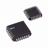
AD1671KP Analog Devices Inc, AD1671KP Datasheet - Page 10

AD1671KP
Manufacturer Part Number
AD1671KP
Description
IC ADC SNGL 12BIT 28PLCC
Manufacturer
Analog Devices Inc
Datasheet
1.AD1671JP.pdf
(16 pages)
Specifications of AD1671KP
Rohs Status
RoHS non-compliant
Number Of Bits
12
Sampling Rate (per Second)
1.25M
Data Interface
Parallel
Number Of Converters
2
Power Dissipation (max)
750mW
Voltage Supply Source
Analog and Digital, Dual ±
Operating Temperature
0°C ~ 70°C
Mounting Type
Surface Mount
Package / Case
28-LCC (J-Lead)
Available stocks
Company
Part Number
Manufacturer
Quantity
Price
Part Number:
AD1671KPZ
Manufacturer:
ADI/亚德诺
Quantity:
20 000
AD1671
UNIPOLAR (0 V TO +2.5 V) CALIBRATION
The connections for the 0 V to +2.5 V input range calibration is
shown in Figure 11. Figure 11 shows an example of how the
offset error can be trimmed in front of the AD1671. The proce-
dure for trimming the offset and gain errors is the same as for
the unipolar 5 V range.
BIPOLAR ( 2.5 V) CALIBRATION
The connections for the bipolar 2.5 V input range is shown in
Figure 12.
OUTPUT LATCHES
Figure 13 shows the AD1671 connected to the 74HC574 octal
D-type edge-triggered latches with 3-state outputs. The latch
can drive highly capacitive loads (i.e., bus lines, I/O ports) while
maintaining the data signal integrity. The maximum setup and
hold times of the 574 type latch must be less than 20 ns (t
–2.5V TO +2.5V
Figure 11. Unipolar (0 V to +2.5 V) Calibration
0 TO +2.5V
GAIN
GAIN
ADJ
ADJ
V
Figure 12. Bipolar ( 2.5 V) Calibration
V
IN
IN
10k
10k
R2
2k
R2
2k
10k
10k
390
390
AD845
AD845
+15V
1k
+15V
1k
R1
R1
1k
OFFSET ADJ
OFFSET ADJ
1k
1µF
1µF
AIN1
AIN2
AIN1
AIN2
SHA OUT
BPO/UPO
REF IN
REF OUT
SHA OUT
BPO/UPO
REF IN
REF OUT
5k
5k
5k
5k
AD1671
AD1671
SHA
SHA
DD
–10–
and t
latch the recommended logic families are S, AS, ALS, F or
BCT. New data from the AD1671 is latched on the rising edge
of the DAV (Pin 16) output pulse. Previous data can be latched
by inverting the DAV output with a 7404 type inverter.
OUT OF RANGE
An out-of-range condition exists when the analog input voltage
is beyond the input range (0 V to +2.5 V, 0 V to +5 V, 2.5 V,
input voltage is within the analog input range. OTR is set HIGH
and will remain HIGH when the analog input voltage exceeds
the input range by typically 1/2 LSB (OTR transition is tested to
codes. OTR will remain HIGH until the analog input is within
the input range and another conversion is completed. By logical
ANDing OTR with the MSB and its complement, overrange
high or underrange low conditions can be detected. Table II is a
truth table for the over/under range circuit in Figure 14. Sys-
tems requiring programmable gain conditioning prior to the
AD1671 can immediately detect an out-of-range condition, thus
eliminating gain selection iterations.
5 V) of the converter OTR (Pin 15) is set low when the analog
6 LSBs of accuracy) from the center of the full-scale output
SS
minimum). To satisfy the requirements of the 574 type
OTR
0
0
1
1
Figure 14. Overrange or Underrange Logic
AD1671
Figure 13. AD1671 to Output Latches
Table II. Out-of-Range Truth Table
MSB
OTR
MSB
BIT 10
BIT 11
BIT 12
BIT 1
BIT 2
BIT 3
BIT 4
BIT 5
BIT 6
BIT 7
BIT 8
BIT 9
DAV
MSB
0
1
0
1
1D
4D
7D
1D
4D
7D
2D
3D
5D
6D
8D
CLOCK
2D
3D
5D
6D
8D
CLOCK
74HC574
74HC574
Analog Input Is
In Range
In Range
Underrange
Overrange
OC
OC
3Q
4Q
5Q
6Q
7Q
8Q
3Q
4Q
5Q
6Q
7Q
8Q
1Q
2Q
1Q
2Q
UNDER = "1"
OVER = "1"
DATA BUS
3-STATE
CONTROL
REV. B


