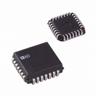
AD1671KP Analog Devices Inc, AD1671KP Datasheet - Page 4

AD1671KP
Manufacturer Part Number
AD1671KP
Description
IC ADC SNGL 12BIT 28PLCC
Manufacturer
Analog Devices Inc
Datasheet
1.AD1671JP.pdf
(16 pages)
Specifications of AD1671KP
Rohs Status
RoHS non-compliant
Number Of Bits
12
Sampling Rate (per Second)
1.25M
Data Interface
Parallel
Number Of Converters
2
Power Dissipation (max)
750mW
Voltage Supply Source
Analog and Digital, Dual ±
Operating Temperature
0°C ~ 70°C
Mounting Type
Surface Mount
Package / Case
28-LCC (J-Lead)
Available stocks
Company
Part Number
Manufacturer
Quantity
Price
Part Number:
AD1671KPZ
Manufacturer:
ADI/亚德诺
Quantity:
20 000
AD1671
Symbol
ACOM
AIN
BIT 1 (MSB)
BIT 2–BIT 11 12-3
BIT 12 (LSB)
BPO/UPO
DAV
DCOM
ENCODE
MSB
OTR
REF COM
REF IN
REF OUT
SHA OUT
V
V
V
TYPE: AI = Analog Input; AO = Analog Output; DI = Digital Input; DO = Digital Outputs; P = Power.
CC
EE
LOGIC
Pin No.
27
22, 23
13
2
26
16
19
17
14
15
20
24
21
25
28
1
18
Type
P
AI
DO
DO
DO
AI
DO
P
DI
DO
DO
AI
AI
AO
AO
P
P
P
Bipolar or Unipolar Configuration Pin. See section on Input Range Connections for details.
Name and Function
Analog Ground.
Analog Inputs, AIN1 and AIN2. The AD1671 can be pin strapped for four input ranges:
Range
0 to +2.5 V, 2.5 V
0 to +5 V, 5 V
Most Significant Bit.
Data Bits 2 through 11.
Least Significant Bit.
Data Available Output. The rising edge of DAV indicates an end of conversion and can be used
to latch current data into an external register. The falling edge of DAV can be used to latch
previous dam into an external register.
Digital Ground.
The analog input is sampled on the rising edge of ENCODE.
Inverted Most Significant Bit. Provides twos complement output data format.
Out of Range is Active HIGH when the analog input is out of range. See Output Data Format,
Table III.
REF COM is the internal reference ground pin. REF COM should be connected as indicated
in the Grounding and Decoupling Rules and Optional External Reference Connection Sections.
REF IN is the external 2.5 V reference input.
REF OUT is the internal 2.5 V reference output.
No Connect for bipolar input ranges. Connect SHA OUT to BPO/UPO for unipolar i n put ranges.
+5 V Analog Power.
–5 V Analog Power.
+5 V Digital Power.
BIT 12 (LSB)
BIT 1 (MSB)
BIT 10
BIT 11
BIT 9
BIT 4
BIT 2
BIT 8
BIT 7
BIT 6
BIT 5
BIT 3
MSB
PIN CONFIGURATION
V
EE
PIN DESCRIPTION
10
11
12
13
14
1
2
3
4
5
6
7
8
9
Pin Strap
Connect AIN1 to AIN2
Connect AIN1 or AIN2 to ACOM
(Not to Scale)
AD1671
TOP VIEW
–4–
27
26
25
24
21
20
18
16
28
23
22
19
17
15
BPO/UPO
SHA OUT
REF IN
REF OUT
REF COM
DCOM
V
ENCODE
OTR
V
ACOM
DAV
AIN1
AIN2
LOGIC
CC
Signal Input
AIN1 or AIN2
AIN1 or AIN2
REV. B


