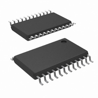
ADC1175CIMTCX/NOPB National Semiconductor, ADC1175CIMTCX/NOPB Datasheet

ADC1175CIMTCX/NOPB
Specifications of ADC1175CIMTCX/NOPB
Available stocks
Related parts for ADC1175CIMTCX/NOPB
ADC1175CIMTCX/NOPB Summary of contents
Page 1
... ADC1175's reference ladder is available for connections, en- abling a wide range of input possibilities. The ADC1175 is offered in a TSSOP designed to operate over the commercial temperature range of -20°C to +75°C. Pin Configuration © 2009 National Semiconductor Corporation ADC1175 Features ■ Internal Sample-and-Hold Function ■ ...
Page 2
Ordering Information Order Code ADC1175CIJM * ADC1175CIJMX * ADC1175CIMTC ADC1175CIMTCX ADC1175EVAL * * Discontinured in the SOIC (EIAJ) package. The Evaluation Board is also discontinued. Shown for reference only. Block Diagram www.national.com Temperature Description −20°C to +75°C SOIC (EIAJ) −20°C ...
Page 3
Pin Descriptions and Equivalent Circuits Pin Symbol No RTS RBS CLK Equivalent Circuit Analog signal input. Conversion range is V Reference Top Bias with ...
Page 4
Pin Symbol No. 3 thru 10 D0- 14 www.national.com Equivalent Circuit Conversion data digital Output pins the LSB ...
Page 5
... Absolute Maximum Ratings If Military/Aerospace specified devices are required, please contact the National Semiconductor Sales Office/ Distributors for availability and specifications Voltage on Any Pin CLK, OE Voltage Digital Output Voltage Input Current (Note 3) Package Input Current (Note 3) Package Dissipation at 25°C ESD Susceptibility (Note 5) ...
Page 6
Symbol Parameter V Reference Top Self Bias Voltage RT Reference Bottom Self Bias V RB Voltage V - RTS Self Bias Voltage Delta V RBS Reference Voltage Delta RT RB Power Supply Characteristics IA Analog Supply Current ...
Page 7
Symbol Parameter SINAD Signal-to- Noise & Distortion SNR Signal-to- Noise Ratio SFDR Spurious Free Dynamic Range THD Total Harmonic Distortion Note 1: Absolute Maximum Ratings indicate limits beyond which damage to the device may occur. Operating Ratings indicate conditions for ...
Page 8
Typical Performance Characteristics INL vs. Temp at f SNR vs. Temp at f THD vs. Temp www.national.com CLK 10009220 CLK 10009222 10009223 8 DNL vs. Temp at f CLK 10009221 SNR vs. Temp at f CLK 10009233 THD vs. Temp ...
Page 9
SINAD/ENOB vs. Temp SINAD and ENOB vs. Clock Duty Cycle SFDR vs. Temp and f IN 10009230 SINAD/ENOB vs. Temp 10009224 SFDR vs. Temp and f 10009225 Differential Gain vs. Temperature 9 10009231 IN 10009229 10009226 www.national.com ...
Page 10
Differential Phase vs. Temperature Specification Definitions ANALOG INPUT BANDWIDTH is a measure of the frequen which the reconstructed output fundamental drops 3 dB below its low frequency value for a full scale input. The test is performed with ...
Page 11
Timing Diagram FIGURE 1. ADC1175 Timing Diagram 10009212 FIGURE Test Circuit EN DIS 11 10009211 www.national.com ...
Page 12
Functional Description The ADC1175 uses a new, unique architecture to achieve 7.2 effective bits at and maintains superior dynamic performance up to ½ the clock frequency. The analog signal at V that is within the voltage range set IN by ...
Page 13
FIGURE 3. Simple, Low Component Count, Self -Bias Reference application. Because of resistor tolerances, the reference voltages can vary by as much as 6%. Choose an amplifier that can drive a dynamic capacitance (see text). 13 10009213 www.national.com ...
Page 14
FIGURE 4. Better defining the ADC Reference Voltage. Self-bias is still used, but the reference voltages are trimmed by providing a small trim current with the operational amplifiers. www.national.com 14 10009214 ...
Page 15
FIGURE 5. Driving the reference to force desired values requires driving with a low impedance source, provided by the transistors. Note that pins 16 and 22 are not connected. 3.0 POWER SUPPLY CONSIDERATIONS Many A/D converters draw sufficient transient current ...
Page 16
THE ADC1175 CLOCK Although the ADC1175 is tested and its performance is guar- anteed with a 20MHz clock, it typically will function with clock frequencies from 1MHz to 30MHz. If continuous conversions are not required, power consump- tion can ...
Page 17
DV and DGND. These large charging current DD spikes can couple into the analog section, degrading dynamic performance. Buffering the digital data outputs (with an 74AC541, for example) may ...
Page 18
Physical Dimensions www.national.com inches (millimeters) unless otherwise noted 24-Lead Package JM Ordering Number ADC1175CIJM NS Package Number M24D 24-Lead Package TC Ordering Number ADC1175CIMTC NS Package Number MTC24 18 ...
Page 19
Notes 19 www.national.com ...
Page 20
... For more National Semiconductor product information and proven design tools, visit the following Web sites at: Products Amplifiers www.national.com/amplifiers Audio www.national.com/audio Clock and Timing www.national.com/timing Data Converters www.national.com/adc Interface www.national.com/interface LVDS www.national.com/lvds Power Management www.national.com/power Switching Regulators www.national.com/switchers LDOs www.national.com/ldo LED Lighting www ...


