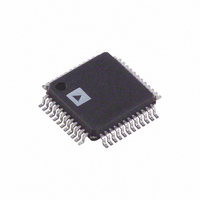
AD7660AST Analog Devices Inc, AD7660AST Datasheet - Page 3

AD7660AST
Manufacturer Part Number
AD7660AST
Description
IC ADC 16BIT UNIPOLAR 48-LQFP
Manufacturer
Analog Devices Inc
Series
PulSAR®r
Datasheet
1.AD7660ASTZRL.pdf
(20 pages)
Specifications of AD7660AST
Rohs Status
RoHS non-compliant
Number Of Bits
16
Sampling Rate (per Second)
100k
Data Interface
Serial, Parallel
Number Of Converters
1
Power Dissipation (max)
25mW
Voltage Supply Source
Analog and Digital
Operating Temperature
-40°C ~ 85°C
Mounting Type
Surface Mount
Package / Case
48-LQFP
For Use With
EVAL-AD7660CBZ - BOARD EVALUATION FOR AD7660
Available stocks
Company
Part Number
Manufacturer
Quantity
Price
Company:
Part Number:
AD7660AST
Manufacturer:
BROADCOM
Quantity:
27
Company:
Part Number:
AD7660AST
Manufacturer:
ADI
Quantity:
300
Company:
Part Number:
AD7660ASTZ
Manufacturer:
ATMEL
Quantity:
36
Company:
Part Number:
AD7660ASTZ
Manufacturer:
ADI
Quantity:
246
Company:
Part Number:
AD7660ASTZ
Manufacturer:
Analog Devices Inc
Quantity:
10 000
Part Number:
AD7660ASTZ
Manufacturer:
ADI/亚德诺
Quantity:
20 000
Company:
Part Number:
AD7660ASTZRL
Manufacturer:
Analog Devices Inc
Quantity:
10 000
Parameter
TEMPERATURE RANGE
NOTES
1
2
3
4
5
6
Specifications subject to change without notice.
TIMING SPECIFICATIONS
Parameter
REFER TO FIGURES 11 AND 12
REFER TO FIGURES 13, 14, AND 15 (Parallel Interface Modes)
REFER TO FIGURE 16 AND 17 (Master Serial Interface Modes)
REFER TO FIGURES 18 AND 20 (Slave Serial Interface Modes)
NOTES
1
2
Specifications subject to change without notice.
REV. D
LSB means least significant bit. With the 0 V to 2.5 V input range, one LSB is 38.15 mV.
Typical rms noise at worst-case transitions and temperatures.
See Definition of Specifications section. These specifications do not include the error contribution from the external reference.
All specifications in dB are referred to a full-scale input FS. Tested with an input signal at 0.5 dB below full-scale unless otherwise specified.
Tested in Parallel Reading Mode.
With all digital inputs forced to DVDD or DGND respectively.
In serial interface modes, the SYNC, SCLK, and SDOUT timings are defined with a maximum load C
If the polarity of SCLK is inverted, the timing references of SCLK are also inverted.
Specified Performance
Convert Pulsewidth
Time between Conversions
CNVST LOW to BUSY HIGH Delay
BUSY HIGH All Modes Except in
Aperture Delay
End of Conversion to BUSY LOW Delay
Conversion Time
Acquisition Time
RESET Pulsewidth
CNVST LOW to DATA Valid Delay
DATA Valid to BUSY LOW Delay
Bus Access Request to DATA Valid
Bus Relinquish Time
CS LOW to SYNC Valid Delay
CS LOW to Internal SCLK Valid Delay
CS LOW to SDOUT Delay
CNVST LOW to SYNC Delay
SYNC Asserted to SCLK First Edge Delay
Internal SCLK Period
Internal SCLK HIGH (INVSCLK Low)
Internal SCLK LOW (INVSCLK Low)
SDOUT Valid Setup Time
SDOUT Valid Hold Time
SCLK Last Edge to SYNC Delay
CS HIGH to SYNC HI-Z
CS HIGH to Internal SCLK HI-Z
CS HIGH to SDOUT HI-Z
BUSY HIGH in Master Serial Read after Convert
CNVST LOW to SYNC Asserted Delay
SYNC Deasserted to BUSY LOW Delay
External SCLK Setup Time
External SCLK Active Edge to SDOUT Delay
SDIN Setup Time
SDIN Hold Time
External SCLK Period
External SCLK HIGH
External SCLK LOW
Master Serial Read after Convert Mode
(–40 C to +85 C, AVDD = DVDD = 5 V, OVDD = 2.7 V to 5.25 V, unless otherwise noted.)
2
2
Conditions
T
MIN
to T
MAX
1
1
–3–
Symbol
t
t
t
t
t
t
t
t
t
t
t
t
t
t
t
t
t
t
t
t
t
t
t
t
t
t
t
t
t
t
t
t
t
t
t
t
t
1
2
3
4
5
6
7
8
9
10
11
12
13
14
15
16
17
18
19
20
21
22
23
24
25
26
27
28
29
30
31
32
33
34
35
36
37
Min
–40
L
of 10 pF; otherwise, the load is 60 pF maximum.
Min
5
10
10
8
10
45
5
4
40
30
9.5
4.5
3
3
5
3
5
5
25
10
10
Typ
Typ
2
500
1.5
50
Max
+85
Max
15
2
2
2
40
15
10
10
10
75
10
10
10
3.2
16
AD7660
Unit
∞C
Unit
ns
ms
ns
ms
ns
ns
ms
ms
ns
ms
ns
ns
ns
ns
ns
ns
ns
ns
ns
ns
ns
ns
ns
ns
ns
ns
ms
ms
ns
ns
ns
ns
ns
ns
ns
ns


