AD872AJE Analog Devices Inc, AD872AJE Datasheet
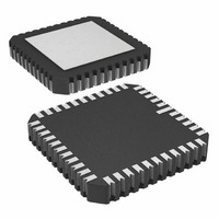
IC ADC 12BIT 10MSPS 44-CLCC

AD872AJE

Manufacturer Part Number
AD872AJE
Description
IC ADC 12BIT 10MSPS 44-CLCC
Manufacturer
Analog Devices Inc
Datasheet

Specifications of AD872AJE

Rohs Status
RoHS non-compliant
Number Of Bits
12
Sampling Rate (per Second)
10M
Data Interface
Parallel
Number Of Converters
7
Power Dissipation (max)
1.3W
Voltage Supply Source
Analog and Digital, Dual ±
Operating Temperature
0°C ~ 70°C
Mounting Type
Surface Mount
Package / Case
44-CLCC

Available stocks

Company
Part Number
Manufacturer
Quantity
Price
Part Number:
AD872AJE
Manufacturer:
a
Quantity:
17
Part Number:
AD872AJE
Manufacturer:
ADI
Quantity:
11
a
PRODUCT DESCRIPTION
The AD872A is a monolithic 12-bit, 10 MSPS analog-to-digital
converter with an on-chip, high performance track-and-hold
amplifier and voltage reference. The AD872A uses a multistage
differential pipelined architecture with error correction logic to
provide 12-bit accuracy at 10 MSPS data rates and guarantees
no missing codes over the full operating temperature range. The
AD872A is a redesigned version of the AD872 which has been
optimized for lower noise. The AD872A is pin compatible with
the AD872, allowing the parts to be used interchangeably as sys-
tem requirements change.
The low noise input track-and-hold (T/H) of the AD872A is
ideally suited for high-end imaging applications. In addition, the
T/H’s high input impedance and fast settling characteristics al-
low the AD872A to easily interface with multiplexed systems
that switch multiple signals through a single A/D converter. The
dynamic performance of the T/H also renders the AD872A suit-
able for sampling single channel inputs at frequencies up to and
beyond the Nyquist rate. The AD872A provides both reference
output and reference input pins, allowing the onboard reference
to serve as a system reference. An external reference can also be
chosen to suit the dc accuracy and temperature drift require-
ments of the application. A single clock input is used to control
all internal conversion cycles. The digital output data is pre-
sented in twos complement binary output format. An out-of-
range signal indicates an overflow condition, and can be used
with the most significant bit to determine low or high overflow.
REV. A
Information furnished by Analog Devices is believed to be accurate and
reliable. However, no responsibility is assumed by Analog Devices for its
use, nor for any infringements of patents or other rights of third parties
which may result from its use. No license is granted by implication or
otherwise under any patent or patent rights of Analog Devices.
FEATURES
Monolithic 12-Bit 10 MSPS A/D Converter
Low Noise: 0.26 LSB RMS Referred-to-Input
No Missing Codes Guaranteed
Differential Nonlinearity Error: 0.5 LSB
Signal-to-Noise and Distortion Ratio: 68 dB
Spurious-Free Dynamic Range: 75 dB
Power Dissipation: 1.03 W
Complete: On-Chip Track-and-Hold Amplifier and
Twos Complement Binary Output Data
Out-of-Range Indicator
28-Lead Ceramic DIP or 44-Terminal Leadless Chip
Voltage Reference
Carrier Package
REF GND
REF OUT
The AD872A is fabricated on Analog Devices’ ABCMOS-l
process that utilizes high speed bipolar and CMOS transistors
on a single chip.
The AD872A is packaged in a 28-lead ceramic DIP and a 44-
terminal leadless ceramic surface mount package (LCC). Opera-
tion is specified from 0 C to +70 C and –55 C to +125 C.
PRODUCT HIGHLIGHTS
The AD872A offers a complete single-chip sampling, 12-bit
10 MSPS analog-to-digital conversion function in a 28-lead DIP
or 44-terminal LCC.
Low Noise—The AD872A features 0.26 LSB rms referred to-
input noise.
Low Power—The AD872A at 1.03 W consumes a fraction of the
power of presently available hybrids.
On-Chip Track-and-Hold (T/H)—The low noise, high imped-
ance T/H input eliminates the need for external buffers and can
be configured for single-ended or differential inputs.
Ease of Use—The AD872A is complete with T/H and voltage
reference and is pin-compatible with the AD872.
Out of Range (OTR)—The OTR output bit indicates when the
input signal is beyond the AD872A’s input range.
One Technology Way, P.O. Box 9106, Norwood, MA 02062-9106, U.S.A.
Tel: 781/329-4700
Fax: 781/326-8703
CLOCK
REF IN
V
V
INA
INB
*
ONLY AVAILABLE ON 44-TERMINAL SURFACE MOUNT PACKAGE
T/H
REFERENCE
AD872A
Complete 12-Bit 10 MSPS
A/D
Monolithic A/D Converter
FUNCTIONAL BLOCK DIAGRAM
+2.5V
4
AV
DAC
DD
World Wide Web Site: http://www.analog.com
AGND
+
T/H
CORRECTION LOGIC
AV
A/D
*
OEN
SS
4
DAC
OTR
DV
© Analog Devices, Inc., 1997
+
OUTPUT BUFFERS
DD
T/H
MSB
DGND
A/D
AD872A
*
3
MSB
*
DAC
DRV
DD
+
BIT2–BIT12
*
DRGND
A/D
4

Related parts for AD872AJE

AD872AJE Summary of contents

Page 1

FEATURES Monolithic 12-Bit 10 MSPS A/D Converter Low Noise: 0.26 LSB RMS Referred-to-Input No Missing Codes Guaranteed Differential Nonlinearity Error: 0.5 LSB Signal-to-Noise and Distortion Ratio Spurious-Free Dynamic Range Power Dissipation: 1.03 W Complete: On-Chip ...

Page 2

AD872A–SPECIFICATIONS DC SPECIFICATIONS ( MIN Parameter RESOLUTION MAX CONVERSION RATE INPUT REFERRED NOISE ACCURACY Integral Nonlinearity (INL) Differential Nonlinearity (DNL) No Missing Codes 2 Zero Error (@ + Gain Error (@ +25 C) TEMPERATURE DRIFT Zero ...

Page 3

AC SPECIFICATIONS ( MIN Parameter SIGNAL-TO-NOISE & DISTORTION RATIO (S/N+ MHz INPUT f = 4.99 MHz INPUT SIGNAL-TO-NOISE RATIO (SNR MHz INPUT f = 4.99 MHz INPUT TOTAL HARMONIC DISTORTION (THD) f ...

Page 4

AD872A SWITCHING SPECIFICATIONS Parameter 1 Clock Period CLOCK Pulsewidth High CLOCK Pulsewidth Low 2 Clock Duty Cycle Output Delay Pipeline Delay (Latency) Data Access Time (LCC Package Only) Output Float Delay (LCC Package Only) NOTES 1 Conversion rate is operational ...

Page 5

DIP LCC Symbol Pin No. Pin No INA INB AGND DGND ...

Page 6

... SPURIOUS FREE DYNAMIC RANGE The difference, in dB, between the rms amplitude of the input signal and the peak spurious signal. ORDERING GUIDE Model Temperature Range AD872AJD +70 C AD872AJE + AD872ASD – +125 C 2 AD872ASE – +125 C NOTES Ceramic DIP Leadless Ceramic Chip Carrier ...

Page 7

Dynamic Characteristics–Sample Rate: 10 MSPS–AD872A INPUT FREQUENCY – Hz Figure 2. AD872A S/(N+D) Input Frequency 1 Figure 4. AD872A Typical FFT Figure 5. ...

Page 8

AD872A–Dynamic Characteristics–Sample Rate: 10 MSPS 700000 618061 600000 500000 400000 300000 200000 100000 19559 0 –1 0 DEVIATION FROM CORRECT CODE – LSB Figure 8. AD872A Output Code Histogram for DC Input f = 750kHz IN f ...

Page 9

THEORY OF OPERATION The AD872A is implemented using a 4-stage pipelined multiple flash architecture. A differential input track-and-hold amplifier (THA) acquires the input and converts the input voltage into a differential current. A 4-bit approximation of the input is made ...

Page 10

AD872A Figure 12 shows the common-mode rejection performance vs. frequency for p-p common-mode input. This excellent common-mode rejection over a wide bandwidth affords the user the opportunity to eliminate many potential sources of input noise as common ...

Page 11

The wide input bandwidth and superior dynamic performance of the input THA make the AD872A suitable for undersam- pling applications where the input frequency exceeds half the sample frequency. The input THA is designed to recover rap- idly from input ...

Page 12

AD872A R 2. REF IN +5V REF 2k 3.9k REF GND Figure 21. Optional +5 V Reference Input Circuit REFERENCE GROUND The REF GND pin provides the reference point for both the reference input, and the reference output. ...

Page 13

Note that if the in- put is driven beyond +1.5 V, the digital outputs may not stay at +FS, but may actually fold back to midscale. The AD872A’s CMOS digital output drivers are sized ...

Page 14

AD872A ANALOG SUPPLIES AND GROUNDS The AD872A features separate analog and digital supply and ground pins, helping to minimize digital corruption of sensitive analog signals. In general, AV and AV SS should be decoupled to AGND, the analog common, as ...

Page 15

Figure 32 shows how a dc offset can be applied using the AD568 12-bit, high speed digital-to-analog converter (DAC). This circuit can be used for applications requiring offset adjust- ments on every clock cycle. The AD568 connection scheme is used ...

Page 16

AD872A +5A C12 0.1 ANALOG IN J1 TP1 R1 C20 10pF 49.9 C18 C7 0 JP1 JP2 U2 C21 REF43 + OUT 5 4 GND * ...

Page 17

Figure 35. Silkscreen Layer PCB Layout (Not Shown to Scale) Reference Designator R1 R4–R17 C1–C3 C4–C6 C7 C8–C19, C22 C20 C21 FB1–FB3 J1, J2 JP2 JP1–JP11 P1 REV. A Table IV. ...

Page 18

AD872A Figure 36. Component Side PCB Layout (Not Shown to Scale) Figure 37. Solder Side PCB Layout (Not Shown to Scale) –18– REV. A ...

Page 19

Figure 38. Ground Layer PCB Layout (Not Shown to Scale) Figure 39. Power Layer PCB Layout (Not Shown to Scale) REV. A –19– AD872A ...

Page 20

AD872A PIN 1 0.225 (5.72) MAX 0.200 (5.08) 0.125 (3.18) OUTLINE DIMENSIONS Dimensions shown in inches and (mm). 28-Lead Side Brazed DIP (D-28) 0.005 (0.13) MIN 0.100 (2.54) MAX 28 15 0.610 (15.49) 0.500 (12.70 0.060 (1.52) 1.490 ...

Related keywords