AD872AJE Analog Devices Inc, AD872AJE Datasheet - Page 5
AD872AJE
Manufacturer Part Number
AD872AJE
Description
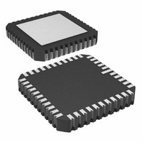
IC ADC 12BIT 10MSPS 44-CLCC
Manufacturer
Analog Devices Inc
Datasheet
1.AD872AJD.pdf
(20 pages)
Specifications of AD872AJE
Rohs Status
RoHS non-compliant
Number Of Bits
12
Sampling Rate (per Second)
10M
Data Interface
Parallel
Number Of Converters
7
Power Dissipation (max)
1.3W
Voltage Supply Source
Analog and Digital, Dual ±
Operating Temperature
0°C ~ 70°C
Mounting Type
Surface Mount
Package / Case
44-CLCC
Available stocks
Company
Part Number
Manufacturer
Quantity
Price


REV. A
Symbol
V
V
AV
AV
AGND
DGND
DV
BIT 12 (LSB)
BIT 2–BIT 11
MSB
OTR
CLK
REF OUT
REF GND
REF IN
DRV
NC
DRGND
OEN
BIT 1
TYPE: AI = Analog Input; AO = Analog Output; DI = Digital Input; DO = Digital Output; P = Power; N/A = Not Available on 28-lead DIP. Only available on
INA
INB
SS
DD
DD
DD
44-terminal surface mount package.
BIT 12 (LSB)
5, 24
6, 23
20
21
N/A
N/A
DIP
Pin No. Pin No.
1
2
3, 25
4
7, 22
8
18–9
19
26
27
28
N/A
N/A
N/A
AGND
DGND
BIT 11
BIT 10
AV
AV
DV
BIT 9
BIT 8
BIT 7
BIT 6
28-Lead Ceramic DIP
V
V
INA
INB
SS
DD
DD
10
11
12
13
14
1
2
3
4
5
6
7
8
9
(Not to Scale)
TOP VIEW
AD872A
1
2
5, 40
6, 38
9, 36
10
16
26–17
29
30
31
41
42
12, 32
3, 4, 7, 8, 14, 15,
28, 35, 37, 39, 44
11, 34
13
27
LCC
33
43
20
19
18
17
16
15
28
27
26
25
24
23
22
21
REF IN
REF GND
REF OUT
AV
AGND
DGND
DV
CLK
OTR
MSB
BIT 2
BIT 3
BIT 4
BIT 5
SS
DD
Type
AI
AI
P
P
P
P
P
DO
DO
DO
DO
DI
AO
AI
AI
P
P
DI
DO
PIN CONFIGURATIONS
PIN DESCRIPTION
Data Bits 2 through 11.
Name and Function
(+) Analog Input Signal on the differential input amplifier.
(–) Analog Input Signal on the differential input amplifier.
–5 V Analog Supply.
+5 V Analog Supply.
Analog Ground.
Digital Ground.
+5 V Digital Supply.
Least Significant Bit.
Inverted Most Significant Bit. Provides twos complement output
data format.
Out of Range is Active HIGH on the leading edge of Code 0 or the
trailing edge of Code 4096. See Output Data Format Table III.
Clock Input. The AD872A will initiate a conversion on the rising
edge of the clock input. See the Timing Diagram for details.
+2.5 V Reference Output. Tie to REF IN for normal operation.
Reference Ground.
Reference Input. +2.5 V input gives 1 V full-scale range.
+5 V Digital Supply for the output drivers.
No Connect.
Digital Ground for the output drivers. (See section on Power Supply
Decoupling for details on DRV
Output Enable. See the Three State Output Timing Diagram for details.
Most Significant Bit.
–5–
BIT 12 (LSB)
DRGND
NC = NO CONNECT
DRV
BIT 11
AGND
DGND
OEN
NC
NC
NC
NC
DD
10
12
13
14
15
16
17
11
7
8
9
18
6
44-Terminal LCC
19
5
DD
20
4
and DRGND.)
21
(NOT TO SCALE)
3
AD872A
TOP VIEW
22
2
23
1
44
24
25
43
26
42
27
41
28
AD872A
40
39
38
37
36
35
34
33
32
31
30
29
NC
AV
NC
AGND
NC
DRGND
DV
DRV
CLK
OTR
MSB
DD
DD
DD
Related parts for AD872AJE
Image
Part Number
Description
Manufacturer
Datasheet
Request
R

Part Number:
Description:
±1.7g Dual-Axis IMEMS Accelerometer Evaluation Board
Manufacturer:
Analog Devices Inc
Datasheet:

Part Number:
Description:
Inertial Sensor Evaluation System
Manufacturer:
Analog Devices Inc
Datasheet:
Part Number:
Description:
Manufacturer:
Analog Devices Inc
Datasheet:
Part Number:
Description:
Manufacturer:
Analog Devices Inc
Datasheet:
Part Number:
Description:
Manufacturer:
Analog Devices Inc
Datasheet:
Part Number:
Description:
Manufacturer:
Analog Devices Inc
Datasheet:
Part Number:
Description:
Manufacturer:
Analog Devices Inc
Datasheet:
Part Number:
Description:
Manufacturer:
Analog Devices Inc
Datasheet:
Part Number:
Description:
Manufacturer:
Analog Devices Inc
Datasheet:
Part Number:
Description:
Manufacturer:
Analog Devices Inc
Datasheet:
Part Number:
Description:
Manufacturer:
Analog Devices Inc
Datasheet:
Part Number:
Description:
Manufacturer:
Analog Devices Inc
Datasheet:
Part Number:
Description:
Manufacturer:
Analog Devices Inc
Datasheet: