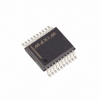
MAX192BEAP+ Maxim Integrated Products, MAX192BEAP+ Datasheet

MAX192BEAP+
Specifications of MAX192BEAP+
Related parts for MAX192BEAP+
MAX192BEAP+ Summary of contents
Page 1
... See last page for Typical Operating Circuit. SPI and QSPI are trademarks of Motorola Corp. Microwire is a trademark of National Semiconductor Corp. ________________________________________________________________ Maxim Integrated Products For free samples & the latest literature: http://www.maxim-ic.com, or phone 1-800-998-8800. For small orders, phone 408-737-7600 ext. 3468. ...
Page 2
Low-Power, 8-Channel, Serial 10-Bit ADC ABSOLUTE MAXIMUM RATINGS V to AGND........................................................... -0.3V to +6V DD AGND to DGND.................................................... -0.3V to +0.3V CH0–CH7 to AGND, DGND ...................... -0. CH0–CH7 Total Input Current.......................................... ±20mA VREF to AGND .......................................... -0.3V to ...
Page 3
ELECTRICAL CHARACTERISTICS (continued ±5 2.0MHz, external clock (50% duty cycle), 15 clocks/conversion cycle (133ksps), 4.7µF capacitor at VREF pin, DD CLK unless otherwise noted. Typical values are ...
Page 4
Low-Power, 8-Channel, Serial 10-Bit ADC ELECTRICAL CHARACTERISTICS (continued ±5 2.0MHz, external clock (50% duty cycle), 15 clocks/conversion cycle (133ksps), 4.7µF capacitor at VREF pin, DD CLK unless otherwise noted. Typical ...
Page 5
TIMING CHARACTERISTICS ( ±5 unless otherwise noted MIN MAX PARAMETER SYMBOL Acquisition Time t DIN to SCLK Setup t DIN to SCLK Hold t SCLK Fall to Output Data Valid ...
Page 6
Low-Power, 8-Channel, Serial 10-Bit ADCs PIN NAME 1–8 CH0–CH7 Sampling Analog Inputs Analog Ground. Also IN- Input for single-enabled conversions. Connect both AGND pins AGND analog ground. Three-Level Shutdown Input. Pulling SHDN low shuts the MAX192 down ...
Page 7
CS 19 SCLK INPUT INT 17 DIN SHIFT CLOCK REGISTER CONTROL 10 SHDN LOGIC 1 CH0 2 CH1 3 CH2 4 ANALOG CH3 T/H INPUT 5 CH4 CLOCK MUX 6 CH5 IN SAR 7 CH6 ADC 8 CH7 REF ...
Page 8
Low-Power, 8-Channel, Serial 10-Bit ADC The T/H enters its tracking mode on the falling clock edge after the fifth bit of the 8-bit control word has been shifted in. The T/H enters its hold mode on the falling clock edge ...
Page 9
Table 2. Channel Selection in Differential Mode (SGL/DIF = 0) SEL2 SEL1 SEL0 CH0 – ...
Page 10
Low-Power, 8-Channel, Serial 10-Bit ADC Table 4a. Unipolar Full Scale and Zero Scale ZERO REFERENCE SCALE Internal Reference 0V at REFADJ 0V External Reference at VREF 0V Table 4b. Differential Bipolar Full Scale, Zero Scale, and Negative Full Scale NEGATIVE ...
Page 11
MAX192 0V TO 4.096V CH7 ANALOG 0.01 F INPUT REFADJ VREF C2 C1 0.01 F 4.7 F +2.5V +2.5V REFERENCE * FULL-SCALE ANALOG INPUT, CONVERSION RESULT = $FFF (HEX) **OPTIONAL. A POTENTIOMETER MAY BE USED IN PLACE OF THE REFERENCE ...
Page 12
Low-Power, 8-Channel, Serial 10-Bit ADC CS t ACQ SCLK 1 4 RB1 UNI/ SGL/ DIN START SEL2 SEL1 SEL0 PD1 BIP DIF SSTRB RB1 DOUT ACQUISITION IDLE A/D STATE 1.5µs (CLK = 2MHz) Figure 6. 24-Bit External Clock Mode Conversion ...
Page 13
CS t SDV SSTRB SCLK Figure 8. External Clock Mode SSTRB Detailed Timing CS SCLK UNI/ DIN START SEL2 SEL1 SEL0 BIP SSTRB DOUT IDLE A/D STATE Figure 9. Internal Clock Mode Timing Most microcontrollers require ...
Page 14
Low-Power, 8-Channel, Serial 10-Bit ADC CS t CSH SSTRB SCLK PD0 CLOCK IN Figure 10. Internal Clock Mode SSTRB Detailed Timing SCLK DIN S CONTROL BYTE 0 DOUT SSTRB Figure 11a. External Clock Mode, 15 Clocks/Conversion Timing ...
Page 15
CLOCK INTERNAL MODE SHDN SETS EXTERNAL CLOCK MODE DIN DOUT DATA VALID ( DATA BITS) MODE POWERED UP Figure 12a. Timing Diagram Power-Down Modes, External Clock CLOCK MODE SETS INTERNAL ...
Page 16
Low-Power, 8-Channel, Serial 10-Bit ADC Table 5. Worst-Case Power-Up Delay Times Reference Reference- Buffer Buffer Compensation Mode Enabled Internal Enabled Internal Enabled External Enabled External Disabled Disabled Table 6. Software Shutdown and Clock Mode PD1 PD0 Device Mode 1 1 ...
Page 17
DIN FULLPD 2.5V REFADJ 0V 4V VREF 0V Figure 13. FULLPD/FASTPD Power-Up Sequence FULL POWER-DOWN 1000 8 CHANNELS 100 1 CHANNEL 10 2ms FASTPD WAIT 400kHz EXTERNAL CLOCK INTERNAL COMPENSATION 1 0 100 200 300 CONVERSIONS PER ...
Page 18
Low-Power, 8-Channel, Serial 10-Bit ADC OUTPUT CODE FULL-SCALE TRANSITION 111 110 101 011 010 001 00 ...
Page 19
F 24k Figure 17. Reference-Adjust Circuit Layout, Grounding, Bypassing For best performance, use printed circuit boards. Wire-wrap boards are not recommended. Board layout should ensure that digital and analog signal lines are separated from each other. ...
Page 20
Low-Power, 8-Channel, Serial 10-Bit ADC 1 CH0 2 CH1 3 CH2 4 ANALOG CH3 MAX192 INPUTS 5 CH4 SSTRB 6 CH5 7 CH6 8 CH7 9 AGND REFADJ 10 SHDN Figure 19. MAX192 QSPI Connection TMS320 to MAX192 Interface Figure ...
Page 21
... This is a shell program for using a stand-alone 68HC16 without any external memory. The internal 1K RAM * is put into bank $0F to maintain 68HC11 code compatibility. This program was written with software * provided in the Motorola 68HC16 Evaluation Kit Roger J.A. Chen, Applications Engineer * MAXIM Integrated Products * November 20, 1992 * ****************************************************************************************************************************************************** INCLUDE ‘EQUATES.ASM’ ;Equates for common reg addrs INCLUDE ‘ ...
Page 22
Low-Power, 8-Channel, Serial 10-Bit ADC LDD #$0800 STD SPCR2 ;set ENDQP to $8 for 9 transfers ***** Initialize QSPI Command RAM ***** LDAA #$80 ;CONT=1,BITSE=0,DT=0,DSCK=0,PCS0=ACTIVE STAA $FD40 ;store first byte in COMMAND RAM LDAA #$C0 ;CONT=1,BITSE=1,DT=0,DSCK=0,PCS0=ACTIVE STAA $FD41 STAA $FD42 ...
Page 23
Figure 21. QSPI Assembly-Code Timing XF CS CLKX SCLK TMS320 CLKR DX DIN DR DOUT FSR SSTRB Figure 22. MAX192 to TMS320 Serial Interface CS SCLK DIN START SEL2 SEL1 SSTRB DOUT Figure 23. TMS320 Serial-Interface Timing Diagram ______________________________________________________________________________________ Low-Power, ...
Page 24
... Maxim cannot assume responsibility for use of any circuitry other than circuitry entirely embodied in a Maxim product. No circuit patent licenses are implied. Maxim reserves the right to change the circuitry and specifications without notice at any time. 24 ____________________Maxim Integrated Products, 120 San Gabriel Drive, Sunnyvale, CA 94086 408-737-7600 © 1997 Maxim Integrated Products ...


