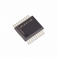
MAX192BEAP+ Maxim Integrated Products, MAX192BEAP+ Datasheet - Page 18

MAX192BEAP+
Manufacturer Part Number
MAX192BEAP+
Description
IC ADC 10BIT SERIAL 20-SSOP
Manufacturer
Maxim Integrated Products
Type
Data Acquisition System (DAS), ADCr
Datasheet
1.MAX192BEWP.pdf
(24 pages)
Specifications of MAX192BEAP+
Resolution (bits)
10 b
Sampling Rate (per Second)
133k
Data Interface
Serial
Voltage Supply Source
Single Supply
Voltage - Supply
±5V
Operating Temperature
-40°C ~ 85°C
Mounting Type
Surface Mount
Package / Case
20-SSOP
Package
20SSOP
Resolution
10 Bit
Sampling Rate
133 KSPS
Architecture
SAR
Number Of Adcs
1
Number Of Analog Inputs
8|4
Digital Interface Type
Serial (4-Wire, SPI, QSPI, Microwire)
Input Type
Voltage
Polarity Of Input Voltage
Unipolar|Bipolar
Conversion Rate
133 KSPs
Interface Type
Serial
Voltage Reference
Internal 4.096 V or External
Supply Voltage (max)
5 V
Maximum Power Dissipation
640 mW
Maximum Operating Temperature
+ 85 C
Mounting Style
SMD/SMT
Minimum Operating Temperature
- 40 C
Lead Free Status / RoHS Status
Lead free / RoHS Compliant
Low-Power, 8-Channel,
Serial 10-Bit ADC
Figure 15. Unipolar Transfer Function, 4.096V = Full Scale
MAX192 is inactive for long periods of time, but where
intermittent bursts of high-speed conversions are
required.
The MAX192 can be used with an internal or external
reference. Diode D1 shown in the Typical Operating
Circuit ensures correct start-up. Any standard signal
diode can be used. An external reference can either be
connected directly at the VREF terminal or at the
REFADJ pin.
The MAX192’s internally trimmed 2.46V reference is
buffered with a gain of 1.678 to scale an external 2.5V
reference at REFADJ to 4.096V at VREF.
The full-scale range of the MAX192 with internal reference
is 4.096V with unipolar inputs, and ±2.048V with differen-
tial bipolar inputs. The internal reference voltage is
adjustable to ±1.5% with the Reference-Adjust Circuit of
Figure 17.
An external reference can be placed at either the
input (REFADJ) or the output (VREF) of the internal
buffer amplifier. The REFADJ input impedance is
18
11 . . . 111
11 . . . 110
00 . . . 011
00 . . . 010
11 . . . 101
00 . . . 001
00 . . . 000
______________________________________________________________________________________
OUTPUT CODE
0
External and Internal References
1
2
INPUT VOLTAGE (LSBs)
3
FULL-SCALE
TRANSITION
External Reference
FS - 3/2LSB
Internal Reference
FS = +4.096V
1LSB = FS
FS
1024
typically 20kΩ. At VREF, the input impedance is a
minimum of 12kΩ for DC currents. During conversion,
an external reference at VREF must be able to deliver
up to 350µA DC load current and have an output
impedance of 10Ω or less. If the reference has higher
output impedance or is noisy, bypass it close to the
VREF pin with a 4.7µF capacitor.
Using the buffered REFADJ input avoids external
buffering of the reference. To use the direct VREF input,
disable the internal buffer by tying REFADJ to V
Figure 15 depicts the nominal, unipolar input/output
(I/O) transfer function, and Figure 16 shows the differ-
ential bipolar input/output transfer function. Code
transitions occur halfway between successive integer
LS B v al ue s. O ut p ut codi ng i s bi nary wi t h
1LSB = 4.00mV (4.096V / 1024) for unipolar operation
and 1LSB = 4.00mV [(4.096V / 2 - -4.096V / 2)/1024]
for bipolar operation.
Figure 17, the Reference-Adjust Circuit, shows how to
adjust the ADC gain in applications that use the internal
reference. The circuit provides ±1.5% (±15LSBs) of
gain adjustment range.
Figure 16. Differential Bipolar Transfer Function,
±4.096V / 2 = Full Scale
011 . . . 111
011 . . . 110
000 . . . 010
000 . . . 001
000 . . . 000
111 . . . 111
111 . . . 110
111 . . . 101
100 . . . 001
100 . . . 000
OUTPUT CODE
Transfer Function and Gain Adjust
-FS
FS = +4.096
1LSB = +4.096
2
1024
DIFFERENTIAL INPUT VOLTAGE (LSBs)
0V
+FS - 1LSB
DD
.


