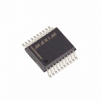
MAX192BEAP+ Maxim Integrated Products, MAX192BEAP+ Datasheet - Page 19

MAX192BEAP+
Manufacturer Part Number
MAX192BEAP+
Description
IC ADC 10BIT SERIAL 20-SSOP
Manufacturer
Maxim Integrated Products
Type
Data Acquisition System (DAS), ADCr
Datasheet
1.MAX192BEWP.pdf
(24 pages)
Specifications of MAX192BEAP+
Resolution (bits)
10 b
Sampling Rate (per Second)
133k
Data Interface
Serial
Voltage Supply Source
Single Supply
Voltage - Supply
±5V
Operating Temperature
-40°C ~ 85°C
Mounting Type
Surface Mount
Package / Case
20-SSOP
Package
20SSOP
Resolution
10 Bit
Sampling Rate
133 KSPS
Architecture
SAR
Number Of Adcs
1
Number Of Analog Inputs
8|4
Digital Interface Type
Serial (4-Wire, SPI, QSPI, Microwire)
Input Type
Voltage
Polarity Of Input Voltage
Unipolar|Bipolar
Conversion Rate
133 KSPs
Interface Type
Serial
Voltage Reference
Internal 4.096 V or External
Supply Voltage (max)
5 V
Maximum Power Dissipation
640 mW
Maximum Operating Temperature
+ 85 C
Mounting Style
SMD/SMT
Minimum Operating Temperature
- 40 C
Lead Free Status / RoHS Status
Lead free / RoHS Compliant
Figure 17. Reference-Adjust Circuit
For best performance, use printed circuit boards.
Wire-wrap boards are not recommended. Board layout
should ensure that digital and analog signal lines are
separated from each other. Do not run analog and digi-
tal (especially clock) lines parallel to one another, or
digital lines underneath the ADC package.
Figure 18 shows the recommended system ground
connections. A single-point analog ground (“star”
ground point) should be established at AGND, sepa-
rate from the logic ground. All other analog grounds
and DGND should be connected to this ground. No
other digital system ground should be connected to
this single-point analog ground. The ground return to
the power supply for this ground should be low imped-
ance and as short as possible for noise-free operation.
High-frequency noise in the V
affect the high-speed comparator in the ADC. Bypass
these supplies to the single-point analog ground with
0.1µF and 4.7µF bypass capacitors close to the
MAX192. Minimize capacitor lead lengths for best sup-
ply-noise rejection. If the +5V power supply is very
noisy, a 10Ω resistor can be connected as a lowpass
filter, as shown in Figure 18.
100k
+5V
24k
Layout, Grounding, Bypassing
______________________________________________________________________________________
510k
0.01 F
DD
12
power supply may
REFADJ
MAX192
The MAX192 can interface with QSPI at high through-
put rates using the circuit in Figure 19. This QSPI circuit
can be programmed to do a conversion on each of the
eight channels. The result is stored in memory without
taxing the CPU since QSPI incorporates its own
micro-sequencer.
Figure 20 details the code that sets up QSPI for
autonomous operation. In external clock mode, the
MAX192 performs a single-ended, unipolar conversion
on each of the eight analog input channels. Figure 21
shows the timing associated with the assembly code of
Figure 20. The first byte clocked into the MAX192 is the
control byte, which triggers the first conversion on CH0.
The last two bytes clocked into the MAX192 are all
zero, and clock out the results of the CH7 conversion.
Figure 18. Power-Supply Grounding Connection
Low-Power, 8-Channel,
* OPTIONAL
V
+5V
DD
R* = 10
Serial 10-Bit ADC
AGND
High-Speed Digital Interfacing
MAX192
SUPPLIES
DGND
+5V
CIRCUITRY
DIGITAL
DGND
GND
19


