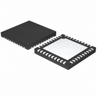
MAX11043ATL+ Maxim Integrated Products, MAX11043ATL+ Datasheet - Page 2

MAX11043ATL+
Manufacturer Part Number
MAX11043ATL+
Description
IC ADC 16BIT W/DAC 40-TQFN-EP
Manufacturer
Maxim Integrated Products
Type
ADC, DACr
Datasheet
1.MAX11043ATL.pdf
(33 pages)
Specifications of MAX11043ATL+
Resolution (bits)
16 b
Sampling Rate (per Second)
9.6M
Data Interface
Serial
Voltage Supply Source
Analog and Digital
Voltage - Supply
3 V ~ 3.6 V
Operating Temperature
-40°C ~ 125°C
Mounting Type
Surface Mount
Package / Case
40-TQFN Exposed Pad
Number Of Converters
4
Conversion Rate
1600 KSPs
Resolution
16 bit
Interface Type
SPI
Voltage Reference
2.5 V
Supply Voltage (max)
3.6 V
Supply Voltage (min)
3 V
Maximum Power Dissipation
2963 mW
Maximum Operating Temperature
+ 125 C
Mounting Style
SMD/SMT
Input Voltage
3.3 V
Minimum Operating Temperature
- 40 C
Lead Free Status / RoHS Status
Lead free / RoHS Compliant
4-Channel, 16-Bit, Simultaneous-Sampling ADCs
with PGA, Filter, and 8-/12-Bit Dual-Stage DAC
ABSOLUTE MAXIMUM RATINGS
AVDD to AGND ....................................................-0.3V to +4.0V
DVDD to DGND .....................................................-0.3V to +4.0V
DVREG to DGND...................................................-0.3V to +3.0V
AGND to DGND.....................................................-0.3V to +0.3V
Analog I/O, REFDACH, REFDACL, REFA, REFB, REFC, REFD,
UP/DWN, CONVRUN, SHDN, DACSTEP, EOC, Digital I/O,
Maximum Current into Any Pin except AVDD, DVDD, DVREG,
ELECTRICAL CHARACTERISTICS
(V
V
C
OSCIN), clock divider set to 4, SHDN = DACSTEP = UP/DWN = DGND, CONVRUN = DVDD, all analog inputs driven directly through
a series 150Ω/330pF anti-alias filter, PGA gain = 1. Default filters and gain settings. DIFF = 1. T
(Note 1). Typical values are at T
Stresses beyond those listed under “Absolute Maximum Ratings” may cause permanent damage to the device. These are stress ratings only, and functional
operation of the device at these or any other conditions beyond those indicated in the operational sections of the specifications is not implied. Exposure to
absolute maximum rating conditions for extended periods may affect device reliability.
2
SIGMA-DELTA ADC
Resolution
Integral Nonlinearity
Differential Nonlinearity
Offset Error
Offset-Error Drift
Gain Error
Gain Temperature Coefficient
Channel Gain-Error Matching
Channel Offset Matching
DYNAMIC PERFORMANCE (PGA Disabled, PGA Gain = 1 x (25kHz -1dB Full-Scale Signal))
Maximum Full-Scale Input
Input-Referred Noise Spectral
Density
Second Harmonic to
Fundamental
Third Harmonic to Fundamental
Spurious-Free Dynamic Range
Channel-to-Channel Isolation
Channel Phase Matching
REFA
REFBP
AVDD
OSCIN, OSCOUT to DGND ....................-0.3V to (DVDD + 0.3V)
AOUT, REFDAC, REFBP to AGND......-0.3V to (AVDD + 0.3V)
AGND, DGND...............................................................±50mA
_______________________________________________________________________________________
= V
= +3.0V to +3.6V, V
= C
REFB
PARAMETER
REFA
= V
= C
REFC
REFB
= V
DVDD
= C
REFD
A
REFC
= +25°C.)
= +3.0V, C
= +2.5V (external reference), V
SYMBOL
= C
SFDR
DNL
INL
OE
GE
N
REFD
DVREG
= C
Guaranteed monotonic
Trimmed with 150Ω/330pF anti-alias filter
Complete analog signal path
Complete analog signal path
ADC modulator gain = 1
100kHz
Unused channels are shorted and
unconnected
Between all channels, including complete
analog signal path
= 10µF, V
REFDAC
= 1µF, f
AGND
CONDITIONS
REFDAC
= V
SCLK
Continuous Power Dissipation (T
Operating Temperature Range .........................-40°C to +125°C
Junction Temperature ......................................................+150°C
Storage Temperature Range ............................-65°C to +150°C
Lead Temperature (soldering, 10s) ................................+300°C
DGND
TQFN Multilayer Board
(derate 37mW/°C above +70°C) ................................2963mW
TQFN Single-Layer Board
(derate 26.3mW/°C above +70°C) ..........................2105.3mW
= V
= 38.4MHz, f
REFDACH
= 0V, common-mode input voltage = AVDD/2, V
= +1.25V (external reference), V
EXCLK
A
= T
= 38.4MHz (external clock applied to
-0.25
MIN
-16
-35
-60
-80
-80
MIN
16
77
85
-1
-1
A
to T
= +70°C)
MAX
-0.05
TYP
-110
±30
±50
108
1.2
-93
±2
85
93
, unless otherwise noted
+0.25
+0.05
MAX
+35
+60
+1
+1
REFDACL
Degrees
ppm/°C
nV/√Hz
UNITS
REFBP
µV/°C
V
LSB
LSB
Bits
mV
mV
dB
dB
dB
dB
%
%
P-P
= 0V,
=


