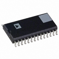
AD974BRZ Analog Devices Inc, AD974BRZ Datasheet - Page 3

AD974BRZ
Manufacturer Part Number
AD974BRZ
Description
IC DAS 16BIT 4CH 200KSPS 28SOIC
Manufacturer
Analog Devices Inc
Type
Data Acquisition System (DAS)r
Datasheet
1.AD974ANZ.pdf
(20 pages)
Specifications of AD974BRZ
Resolution (bits)
16 b
Data Interface
Serial
Sampling Rate (per Second)
200k
Voltage Supply Source
Analog and Digital
Voltage - Supply
5V
Operating Temperature
-40°C ~ 85°C
Mounting Type
Surface Mount
Package / Case
28-SOIC (7.5mm Width)
Sampling Rate
200kSPS
Input Channel Type
Single Ended
Supply Voltage Range - Analog
4.75V To 5.25V
Package
28SOIC W
Resolution
16 Bit
Number Of Adcs
1
Number Of Analog Inputs
4
Digital Interface Type
Serial (SPI)
Input Type
Voltage
Signal To Noise Ratio
85(Min) dB
Polarity Of Input Voltage
Unipolar|Bipolar
Lead Free Status / RoHS Status
Lead free / RoHS Compliant
For Use With
EVAL-AD974CB - BOARD EVAL FOR AD974
Lead Free Status / RoHS Status
Lead free / RoHS Compliant, Lead free / RoHS Compliant
Available stocks
Company
Part Number
Manufacturer
Quantity
Price
Part Number:
AD974BRZ
Manufacturer:
ADI/亚德诺
Quantity:
20 000
Parameter
DIGITAL OUTPUTS
POWER SUPPLIES
TEMPERATURE RANGE
NOTES
1
2
3
4
5
6
7
Specifications subject to change without notice.
TIMING SPECIFICATIONS
Parameter
Convert Pulsewidth
R/C, CS to BUSY Delay
BUSY LOW Time
BUSY Delay after End of Conversion
Aperture Delay
Conversion Time
Acquisition Time
Throughput Time
R/C Low to DATACLK Delay
DATACLK Period
DATA Valid Setup Time
DATA Valid Hold Time
EXT. DATACLK Period
EXT. DATACLK HIGH
EXT. DATACLK LOW
R/C, CS to EXT. DATACLK Setup Time
R/C to CS Setup Time
EXT. DATACLK to SYNC Delay
EXT. DATACLK to DATA Valid Delay
CS to EXT. DATACLK Rising Edge Delay
Previous DATA Valid after CS, R/C Low
BUSY to EXT. DATACLK Setup Time
Final EXT. DATACLK to BUSY Rising Edge
A0, A1 to WR1, WR2 Setup Time
A0, A1 to WR1, WR2 Hold Time
WR1, WR2 Pulsewidth
Specifications subject to change without notic e.
REV. A
LSB means Least Significant Bit. With a 10 V input, one LSB is 305 V.
Typical rms noise at worst case transitions and temperatures.
Full-Scale Error is expressed as the % difference between the actual full-scale code transition voltage and the ideal full-scale transition voltage, and includes the effect
of offset error. For bipolar input, the Full-Scale Error is the worst case of either the –Full-Scale or +Full-Scale code transition voltage errors. For unipolar input
ranges, Full-Scale Error is with respect to the +Full-Scale code transition voltage.
External 2.5 V reference connected to REF.
All specifications in dB are referred to a full-scale 10 V input.
Full-Power Bandwidth is defined as full-scale input frequency at which Signal-to-(Noise + Distortion) degrades to 60 dB, or 10 bits of accuracy.
Recovers to specified performance after a 2
Data Format
Data Coding
Output Capacitance
Leakage Current
Specified Performance
Power Dissipation
Specified Performance
V
V
V
V
I
I
PWRD LOW
PWRD HIGH
DIG
ANA
OL
OH
DIG
ANA
Conditions
I
I
High-Z State
High-Z State
V
T
FS input overvoltage.
SINK
SOURCE
OUT
MIN
(f
S
= 200 kHz, V
= 1.6 mA
to T
= 0 V to V
= 500 A
MAX
DIG
DIG
Symbol
t
t
t
t
t
t
t
t
t
t
t
t
t
t
t
t
t
t
t
t
t
t
t
t
t
t
= V
1
2
3
4
5
6
7
6
8
9
10
11
12
13
14
15
16
17
18
19
20
21
22
23
24
25
+ t
ANA
7
= +5 V, –40 C to +85 C)
Min
+4
+4.75
+4.75
–40
–3–
A Grade
Typ
+5
+5
4.5
14
50
Min
50
1.0
50
20
66
20
30
20
10
15
25
10
3.5
5
10
10
50
Max
+0.4
15
+5.25
+5.25
120
+85
5
Serial 16 Bits
Straight Binary
Typ
50
40
3.8
220
220
Min
+4
+4.75 +5
+4.75 +5
–40
B Grade
Typ
4.5
14
50
Max
100
4.0
4.0
5
t
66
66
1.7
12
+ 5
Max
+0.4
15
+5.25
+5.25
120
+85
5
Units
V
V
pF
V
V
mA
mA
mW
AD974
Units
ns
ns
ns
ns
ns
ns
ns
ns
ns
ns
ns
ns
ns
ns
ns
ns
ns
ns
ns
ns
C
A
W
s
s
s
s
s
s


