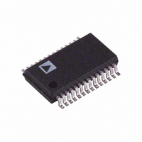
AD974BRS Analog Devices Inc, AD974BRS Datasheet - Page 15

AD974BRS
Manufacturer Part Number
AD974BRS
Description
IC DAS 16BIT 4CH 200KSPS 28-SSOP
Manufacturer
Analog Devices Inc
Type
Data Acquisition System (DAS)r
Datasheet
1.AD974ANZ.pdf
(20 pages)
Specifications of AD974BRS
Rohs Status
RoHS non-compliant
Resolution (bits)
16 b
Sampling Rate (per Second)
200k
Data Interface
Serial
Voltage Supply Source
Analog and Digital
Voltage - Supply
5V
Operating Temperature
-40°C ~ 85°C
Mounting Type
Surface Mount
Package / Case
28-SSOP
Package
28SSOP
Resolution
16 Bit
Sampling Rate
200 KSPS
Number Of Adcs
1
Number Of Analog Inputs
4
Digital Interface Type
Serial (SPI)
Input Type
Voltage
Signal To Noise Ratio
85(Min) dB
Polarity Of Input Voltage
Unipolar|Bipolar
For Use With
EVAL-AD974CB - BOARD EVAL FOR AD974
Available stocks
Company
Part Number
Manufacturer
Quantity
Price
Part Number:
AD974BRS
Manufacturer:
ADI/亚德诺
Quantity:
20 000
OFFSET AND GAIN ADJUSTMENT
The AD974 is factory trimmed to minimize gain, offset and
linearity errors. There are no internal provisions to allow for any
further adjustment of offset error through external circuitry.
The reference of the AD974 can be adjusted as shown in Figure
12. This will allow the full-scale error of any one channel to be
adjusted to zero or will allow the average full-scale error of the
four channels to be minimized.
VOLTAGE REFERENCE
The AD974 has an on-chip temperature compensated bandgap
voltage reference that is factory trimmed to +2.5 V
The accuracy of the AD974 over the specified temperature
range is dominated by the drift performance of the voltage refer-
ence. The on-chip voltage reference is laser-trimmed to provide
a typical drift of 7 ppm/ C. This typical drift characteristic is
shown in Figure 13, which is a plot of the change in reference
voltage (in mV) versus the change in temperature—notice the
plot is normalized for zero error at +25 C. If improved drift perfor-
mance is required, an external reference such as the AD780
should be used to provide a drift as low as 3 ppm/ C. In order to
simplify the drive requirements of the voltage reference (internal
or external), an on-chip reference buffer is provided.
The output of this buffer is provided at the CAP pin and is
available to the user; however, when externally loading the refer-
ence buffer, it is important to make sure that proper precautions
REV. A
Figure 12. AD974 Full-Scale Trim
50k
+5V
Figure 13. Reference Drift
–55
576k
2.2 F
2.2 F
DEGREES – Celsius
+
+
25
REF
AGND2
CAP
AD974
125
20 mV.
–15–
are taken to minimize any degradation in the ADC’s perfor-
mance. Figure 14 shows the load regulation of the reference
buffer. Notice that this figure is also normalized so that there is
zero error with no dc load. In the linear region, the output imped-
ance at this point is typically 1 . Because of this output imped-
ance, it is important to minimize any ac- or input-dependent
loads that will lead to increased distortion. Any dc load will
simply act as a gain error. Although the typical characteristic of
Figure 14 shows that the AD974 is capable of driving loads
greater than 15 mA, it is recommended that the steady state
current not exceed 2 mA.
Using an External Reference
In addition to the on-chip reference, an external 2.5 V reference
can be applied. When choosing an external reference for a
16-bit application, however, careful attention should be paid to
noise and temperature drift. These critical specifications can
have a significant effect on the ADC performance.
Figure 15 shows the AD974 used in bipolar mode with the
AD780 voltage reference applied to the REF pin. The AD780
is a bandgap reference that exhibits ultralow drift, low initial
error and low output noise. For low power applications, the
AD780 provides a low quiescent current, high accuracy and low
temperature drift solution.
Figure 15. External Reference to AD974 Configured for
10 V Input Range
+5V
0.1 F
Figure 14. CAP Pin Load Regulation
3
2
TEMP
V
IN
AD780
SOURCE CAPABILITY
V
GND
OUT
LOAD CURRENT – 5mA/DIV
6
4
–
+
C3
1 F
+
–
C1
2.2 F
2.2 F
V
SINK CAPABILITY
IN
C2
C4
0.1 F
+
–
VxB
VxA
REF
AGND1
AGND2
BIP
V
CAP
ANA
AD974
AD974


