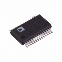
AD974BRS Analog Devices Inc, AD974BRS Datasheet - Page 7

AD974BRS
Manufacturer Part Number
AD974BRS
Description
IC DAS 16BIT 4CH 200KSPS 28-SSOP
Manufacturer
Analog Devices Inc
Type
Data Acquisition System (DAS)r
Datasheet
1.AD974ANZ.pdf
(20 pages)
Specifications of AD974BRS
Rohs Status
RoHS non-compliant
Resolution (bits)
16 b
Sampling Rate (per Second)
200k
Data Interface
Serial
Voltage Supply Source
Analog and Digital
Voltage - Supply
5V
Operating Temperature
-40°C ~ 85°C
Mounting Type
Surface Mount
Package / Case
28-SSOP
Package
28SSOP
Resolution
16 Bit
Sampling Rate
200 KSPS
Number Of Adcs
1
Number Of Analog Inputs
4
Digital Interface Type
Serial (SPI)
Input Type
Voltage
Signal To Noise Ratio
85(Min) dB
Polarity Of Input Voltage
Unipolar|Bipolar
For Use With
EVAL-AD974CB - BOARD EVAL FOR AD974
Available stocks
Company
Part Number
Manufacturer
Quantity
Price
Part Number:
AD974BRS
Manufacturer:
ADI/亚德诺
Quantity:
20 000
CONVERSION CONTROL
The AD974 is controlled by two signals: R/C and CS. When
R/C is brought low, with CS low, for a minimum of 50 ns, the
input signal will be held on the internal capacitor array and a
conversion “n” will begin. Once the conversion process does
begin, the BUSY signal will go low until the conversion is com-
plete. Internally, the signals R/C and CS are ORed together and
there is no requirement on which signal is taken low first when
initiating a conversion. The only requirement is that there be at
least 10 ns of delay between the two signals being taken low.
After the conversion is complete, the BUSY signal will return
high and the AD974 will again resume tracking the input signal.
Under certain conditions the CS pin can be tied Low and R/C
will be used to determine whether you are initiating a conver-
sion or reading data. On the first conversion, after the AD974 is
powered up, the DATA output will be indeterminate.
Conversion results can be clocked serially, using either an
internal clock generated by the AD974 or an external clock.
The AD974 is configured for the internal data clock mode by
pulling the EXT/INT pin low. It is configured for the external
clock mode by pulling the EXT/INT pin high.
REV. A
Figure 3. Serial Data Timing for Reading Previous Conversion Results with Internal Clock
( CS and EXT/ INT Set to Logic Low)
WR1, WR2
DATACLK
CS, R/C
A0, A1
MODE
BUSY
BUSY
DATA
R/C
ACQUIRE
t
2
t
1
t
5
t
8
Figure 2. Basic Conversion Timing
t
10
t
2
t
1
VALID
MSB
1
t
9
CONVERT
BIT 14
VALID
t
11
–7–
2
t
6
t
INTERNAL DATA CLOCK MODE
The AD974 is configured to generate and provide the data clock
when the EXT/INT pin is held low. Typically CS will be tied
low and R/C will be used to initiate a conversion “n.” During
the conversion the AD974 will output 16 bits of data, MSB first,
from conversion “n-1” on the DATA pin. This data will be
synchronized with 16 clock pulses provided on the DATACLK
pin. The output data will be valid on both the rising and falling
edge of the data clock as shown in Figure 3. After the LSB has
been presented, the DATACLK pin will stay low until another
conversion is initiated.
In this mode, the digital input/output pins’ transitions are suit-
ably positioned to minimize degradation on the conversion
result, mainly during the second half of the conversion process.
EXTERNAL DATA CLOCK MODE
The AD974 is configured to accept an externally supplied data
clock when the EXT/INT pin is held high. This mode of opera-
tion provides several methods by which conversion results can
be read. The output data from conversion “n-1” can be read
during conversion “n,” or the output data from conversion “n”
3
BIT 13
VALID
t
6
3
t
23
t
25
t
t
4
24
ACQUIRE
t
VALID
BIT 1
7
15
VALID
LSB
16
CONVERT
AD974


