LM12458CIVX/NOPB National Semiconductor, LM12458CIVX/NOPB Datasheet - Page 23
LM12458CIVX/NOPB
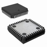
Manufacturer Part Number
LM12458CIVX/NOPB
Description
IC DATA AQUIS SYS 12BIT 44-PLCC
Manufacturer
National Semiconductor
Type
Data Acquisition System (DAS)r
Datasheet
1.LM12458CIVNOPB.pdf
(36 pages)
Specifications of LM12458CIVX/NOPB
Resolution (bits)
12 b
Sampling Rate (per Second)
140k
Data Interface
Parallel
Voltage Supply Source
Analog and Digital
Voltage - Supply
3 V ~ 5.5 V
Operating Temperature
-40°C ~ 85°C
Mounting Type
Surface Mount
Package / Case
44-PLCC
Lead Free Status / RoHS Status
Lead free / RoHS Compliant
Other names
*LM12458CIVX
*LM12458CIVX/NOPB
LM12458CIVX
*LM12458CIVX/NOPB
LM12458CIVX
Available stocks
Company
Part Number
Manufacturer
Quantity
Price
Company:

Part Number:
LM12458CIVX/NOPB
Manufacturer:
Texas Instruments
Quantity:
10 000


1.0 Functional Description
The LM12454 and LM12(H)458 are multi-functional Data
Acquisition Systems that include a fully differential 12-bit-
plus-sign self-calibrating analog-to-digital converter (ADC)
with a two’s-complement output format, an 8-channel
(LM12(H)458) or a 4-channel (LM12454) analog multiplexer,
an internal 2.5V reference, a first-in-first-out (FIFO) register
that can store 32 conversion results, and an Instruction RAM
that can store as many as eight instructions to be sequen-
tially executed. The LM12454 also has a differential multi-
plexer output and a differential S/H input. All of this circuitry
operates on only a single +5V power supply.
The LM12(H)454/8 have three modes of operation:
The fully differential 12-bit-plus-sign ADC uses a charge
redistribution topology that includes calibration capabilities.
Charge re-distribution ADCs use a capacitor ladder in place
of a resistor ladder to form an internal DAC. The DAC is used
by a successive approximation register to generate interme-
diate voltages between the voltages applied to V
V
the sampled analog input voltage as each bit is generated.
The number of intermediate voltages and comparisons
equals the ADC’s resolution. The correction of each bit’s
accuracy is accomplished by calibrating the capacitor ladder
used in the ADC.
Two different calibration modes are available; one compen-
sates for offset voltage, or zero error, while the other corrects
both offset error and the ADC’s linearity error.
When correcting offset only, the offset error is measured
once and a correction coefficient is created. During the full
calibration, the offset error is measured eight times, aver-
aged, and a correction coefficient is created. After comple-
tion of either calibration mode, the offset correction coeffi-
cient is stored in an internal offset correction register.
The LM12(H)454/8’s overall linearity correction is achieved
by correcting the internal DAC’s capacitor mismatch. Each
capacitor is compared eight times against all remaining
smaller value capacitors and any errors are averaged. A
correction coefficient is then created and stored in one of the
thirteen internal linearity correction registers. An internal
state machine, using patterns stored in an internal 16 x 8-bit
ROM, executes each calibration algorithm.
Once calibrated, an internal arithmetic logic unit (ALU) uses
the offset correction coefficient and the 13 linearity correction
coefficients to reduce the conversion’s offset error and lin-
earity error, in the background, during the 12-bit + sign
conversion. The 8-bit + sign conversion and comparison
modes use only the offset coefficient. The 8-bit + sign mode
performs a conversion in less than half the time used by the
12-bit + sign conversion mode.
REF+
12-bit + sign with correction
8-bit + sign without correction
8-bit + sign comparison mode (“watchdog” mode)
. These intermediate voltages are compared against
REF−
and
23
The LM12(H)454/8’s “watchdog” mode is used to monitor a
single-ended or differential signal’s amplitude. Each
sampled signal has two limits. An interrupt can be generated
if the input signal is above or below either of the two limits.
This allows interrupts to be generated when analog voltage
inputs are “inside the window” or, alternatively, “outside the
window”. After a “watchdog” mode interrupt, the processor
can then request a conversion on the input signal and read
the signal’s magnitude.
The analog input multiplexer can be configured for any com-
bination of single-ended or fully differential operation. Each
input is referenced to ground when a multiplexer channel
operates in the single-ended mode. Fully differential analog
input channels are formed by pairing any two channels
together.
The LM12454’s multiplexer outputs and S/H inputs (MUX-
OUT+, MUXOUT− and S/H IN+, S/H IN−) provide the option
for additional analog signal processing. Fixed-gain amplifi-
ers, programmable-gain amplifiers, filters, and other pro-
cessing circuits can operate on the signal applied to the
selected multiplexer channel(s). If external processing is not
used, connect MUXOUT+ to S/H IN+ and MUXOUT− to
S/H IN−.
The LM12(H)454/8’s internal S/H is designed to operate at
its minimum acquisition time (1.13 µs, 12 bits) when the
source impedance, R
increased to a maximum of 4.88 µs (12 bits, f
See Section 2.1 (Instruction RAM “00”) Bits 12–15 for more
information.
An internal 2.5V bandgap reference output is available at pin
44. This voltage can be used as the ADC reference for
ratiometric conversion or as a virtual ground for front-end
analog conditioning circuits. The V
bypassed to ground with a 100 µF capacitor.
Microprocessor overhead is reduced through the use of the
internal conversion FIFO. Thirty-two consecutive conver-
sions can be completed and stored in the FIFO without any
microprocessor intervention. The microprocessor can, at any
time, interrogate the FIFO and retrieve its contents. It can
also wait for the LM12(H)454/8 to issue an interrupt when
the FIFO is full or after any number (≤32) of conversions
have been stored.
Conversion sequencing, internal timer interval, multiplexer
configuration, and many other operations are programmed
and set in the Instruction RAM.
A diagnostic mode is available that allows verification of the
LM12(H)458’s operation. The diagnostic mode is disabled in
the LM12454. This mode internally connects the voltages
present at the V
internal V
setting the Diagnostic bit (Bit 11) in the Configuration register
to a “1”. More information concerning this mode of operation
can be found in Section 2.2.
<
R
S
≤ 4.17 kΩ, the internal S/H’s acquisition time can be
IN+
and V
REFOUT
IN−
S
, is ≤ 60Ω (f
S/H inputs. This mode is activated by
, V
REF+
, V
REF−
CLK
REFOUT
, and GND pins to the
≤ 8 MHz). When 60Ω
pin should be
CLK
www.national.com
= 8 MHz).
Related parts for LM12458CIVX/NOPB
Image
Part Number
Description
Manufacturer
Datasheet
Request
R

Part Number:
Description:
A/D Converter (A-D) IC
Manufacturer:
National Semiconductor
Datasheet:

Part Number:
Description:
IC ACQUISITION SYS 12BIT 44-PLCC
Manufacturer:
National Semiconductor
Datasheet:

Part Number:
Description:
12-Bit + Sign Data Acquisition System with Self-Calibration
Manufacturer:
National Semiconductor
Datasheet:
Part Number:
Description:
National Semiconductor [8-Bit D/A Converter]
Manufacturer:
National Semiconductor
Datasheet:
Part Number:
Description:
National Semiconductor [Media Coprocessor]
Manufacturer:
National Semiconductor
Datasheet:
Part Number:
Description:
Digitally Controlled Tone and Volume Circuit with Stereo Audio Power Amplifier, Microphone Preamp Stage and National 3D Sound
Manufacturer:
National Semiconductor
Datasheet:
Part Number:
Description:
Digitally Controlled Tone and Volume Circuit with Stereo Audio Power Amplifier, Microphone Preamp Stage and National 3D Sound
Manufacturer:
National Semiconductor
Datasheet:
Part Number:
Description:
AC97 Rev 2 Codec with Sample Rate Conversion and National 3D Sound
Manufacturer:
National Semiconductor
Part Number:
Description:
Manufacturer:
National Semiconductor
Datasheet:
Part Number:
Description:
Manufacturer:
National Semiconductor
Datasheet:
Part Number:
Description:
General Purpose, Low Voltage, Low Power, Rail-to-Rail Output Operational Amplifiers
Manufacturer:
National Semiconductor
Datasheet:
Part Number:
Description:
8-bit 20 MSPS flash A/D converter.
Manufacturer:
National Semiconductor
Datasheet:
Part Number:
Description:
Low Noise Quad Operational Amplifier
Manufacturer:
National Semiconductor
Datasheet:
Part Number:
Description:
Quad Differential Line Receivers
Manufacturer:
National Semiconductor
Datasheet: