LM12458CIVX/NOPB National Semiconductor, LM12458CIVX/NOPB Datasheet - Page 27
LM12458CIVX/NOPB
Manufacturer Part Number
LM12458CIVX/NOPB
Description
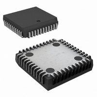
IC DATA AQUIS SYS 12BIT 44-PLCC
Manufacturer
National Semiconductor
Type
Data Acquisition System (DAS)r
Datasheet
1.LM12458CIVNOPB.pdf
(36 pages)
Specifications of LM12458CIVX/NOPB
Resolution (bits)
12 b
Sampling Rate (per Second)
140k
Data Interface
Parallel
Voltage Supply Source
Analog and Digital
Voltage - Supply
3 V ~ 5.5 V
Operating Temperature
-40°C ~ 85°C
Mounting Type
Surface Mount
Package / Case
44-PLCC
Lead Free Status / RoHS Status
Lead free / RoHS Compliant
Other names
*LM12458CIVX
*LM12458CIVX/NOPB
LM12458CIVX
*LM12458CIVX/NOPB
LM12458CIVX
Available stocks
Company
Part Number
Manufacturer
Quantity
Price
Company:

Part Number:
LM12458CIVX/NOPB
Manufacturer:
Texas Instruments
Quantity:
10 000


2.0 Internal User-Programmable
Registers
Bits 12–15 are used to store the user-programmable acqui-
sition time. The Sequencer keeps the internal S/H in the
acquisition mode for a fixed number of clock cycles (nine
clock cycles, for 12-bit + sign conversions and two clock
cycles for 8-bit + sign conversions or “watchdog” compari-
sons) plus a variable number of clock cycles equal to twice
the value stored in Bits 12–15. Thus, the S/H’s acquisition
time is (9 + 2D) clock cycles for 12-bit + sign conversions
and (2 + 2D) clock cycles for 8-bit + sign conversions or
“watchdog” comparisons, where D is the value stored in Bits
12–15. The minimum acquisition time compensates for the
typical internal multiplexer series resistance of 2 kΩ, and any
additional delay created by Bits 12–15 compensates for
source resistances greater than 60Ω (100Ω). (For this acqui-
sition time discussion, numbers in ( ) are shown for the
LM12(H)454/8 operating at 5 MHz.) The necessary acquisi-
tion time is determined by the source impedance at the
multiplexer input. If the source resistance (R
and the clock frequency is 8 MHz, the value stored in bits
12–15 (D) can be 0000. If R
equations determine the value that should be stored in
bits 12–15.
for 12-bits + sign
for 8-bits + sign and “watchdog”
R
higher integer value. If D is greater than 15, it is advisable to
lower the source impedance by using an analog buffer be-
tween the signal source and the LM12(H)458’s multiplexer
inputs. The value of D can also be used to compensate for
the settling or response time of external processing circuits
connected between the LM12454’s MUXOUT and S/H IN
pins.
Instruction RAM “01”
The second Instruction RAM section is selected by placing a
“01” in Bits 8 and 9 of the Configuration register.
Bits 0–7 hold “watchdog” limit #1. When Bit 11 of Instruction
RAM “00” is set to a “1”, the LM12(H)454/8 performs a
“watchdog” comparison of the sampled analog input signal
with the limit #1 value first, followed by a comparison of the
same sampled analog input signal with the value found in
limit #2 (Instruction RAM “10”).
Bit 8 holds limit #1’s sign.
Bit 9’s state determines the limit condition that generates a
“watchdog” interrupt. A “1” causes a voltage greater than
limit #1 to generate an interrupt, while a “0” causes a voltage
less than limit #1 to generate an interrupt.
Bits 10–15 are not used.
Instruction RAM “10”
The third Instruction RAM section is selected by placing a
“10” in Bits 8 and 9 of the Configuration register.
Bits 0–7 hold “watchdog” limit #2. When Bit 11 of Instruction
RAM “00” is set to a “1”, the LM12(H)454/8 performs a
“watchdog” comparison of the sampled analog input signal
with the limit #1 value first (Instruction RAM “01”), followed
by a comparison of the same sampled analog input signal
with the value found in limit #2.
Bit 8 holds limit #2’s sign.
S
is in kΩ and f
CLK
(Continued)
D = 0.45 x R
D = 0.36 x R
is in MHz. Round the result to the next
S
>
S
S
60Ω (100Ω), the following
x f
x f
CLK
CLK
S
)
<
60Ω (100Ω)
27
Bit 9 ’s state determines the limit condition that generates a
“watchdog” interrupt. A “1” causes a voltage greater than
limit #2 to generate an interrupt, while a “0” causes a voltage
less than limit #2 to generate an interrupt.
Bits 10–15 are not used.
2.2 CONFIGURATION REGISTER
The Configuration register, 1000 (A4–A1, BW = 0) or 1000x
(A4–A0, BW = 1) is a 16-bit control register with read/write
capability. It acts as the LM12454’s and LM12(H)458’s “con-
trol panel” holding global information as well as start/stop,
reset, self-calibration, and stand-by commands.
Bit 0 is the START/STOP bit. Reading Bit 0 returns an
indication of the Sequencer’s status. A “0” indicates that the
Sequencer is stopped and waiting to execute the next in-
struction. A “1” shows that the Sequencer is running. Writing
a “0” halts the Sequencer when the current instruction has
finished execution. The next instruction to be executed is
pointed to by the instruction pointer found in the status
register. A “1” restarts the Sequencer with the instruction
currently pointed to by the instruction pointer. (See Bits 8–10
in the Interrupt Status register.)
Bit 1 is the LM12(H)454/8’s system RESET bit. Writing a “1”
to Bit 1 stops the Sequencer (resetting the Configuration
register’s START/STOP bit), resets the Instruction pointer to
“000” (found in the Interrupt Status register), clears the Con-
version FIFO, and resets all interrupt flags. The RESET bit
will return to “0” after two clock cycles unless it is forced high
by writing a “1” into the Configuration register’s Standby bit.
A reset signal is internally generated when power is first
applied to the part. No operation should be started until the
RESET bit is “0”.
Writing a “1” to Bit 2 initiates an auto-zero offset voltage
calibration. Unlike the eight-sample auto-zero calibration
performed during the full calibration procedure, Bit 2 initiates
a “short” auto-zero by sampling the offset once and creating
a correction coefficient (full calibration averages eight
samples of the converter offset voltage when creating a
correction coefficient). If the Sequencer is running when Bit 2
is set to “1”, an auto-zero starts immediately after the con-
clusion of the currently running instruction. Bit 2 is reset
automatically to a “0” and an interrupt flag (Bit 3, in the
Interrupt Status register) is set at the end of the auto-zero
(76 clock cycles). After completion of an auto-zero calibra-
tion, the Sequencer fetches the next instruction as pointed to
by the Instruction RAM’s pointer and resumes execution. If
the Sequencer is stopped, an auto-zero is performed imme-
diately at the time requested.
Writing a “1” to Bit 3 initiates a complete calibration process
that includes a “long” auto-zero offset voltage correction (this
calibration averages eight samples of the comparator offset
voltage when creating a correction coefficient) followed by
an ADC linearity calibration. This complete calibration is
started after the currently running instruction is completed if
the Sequencer is running when Bit 3 is set to “1”. Bit 3 is
reset automatically to a “0” and an interrupt flag (Bit 4, in the
Interrupt Status register) will be generated at the end of the
calibration procedure (4944 clock cycles). After completion
of a full auto-zero and linearity calibration, the Sequencer
fetches the next instruction as pointed to by the Instruction
RAM’s pointer and resumes execution. If the Sequencer is
stopped, a full calibration is performed immediately at the
time requested.
Bit 4 is the Standby bit. Writing a “1” to Bit 4 immediately
places the LM12(H)454/8 in Standby mode. Normal opera-
tion returns when Bit 4 is reset to a “0”. The Standby com-
www.national.com
Related parts for LM12458CIVX/NOPB
Image
Part Number
Description
Manufacturer
Datasheet
Request
R

Part Number:
Description:
A/D Converter (A-D) IC
Manufacturer:
National Semiconductor
Datasheet:

Part Number:
Description:
IC ACQUISITION SYS 12BIT 44-PLCC
Manufacturer:
National Semiconductor
Datasheet:

Part Number:
Description:
12-Bit + Sign Data Acquisition System with Self-Calibration
Manufacturer:
National Semiconductor
Datasheet:
Part Number:
Description:
National Semiconductor [8-Bit D/A Converter]
Manufacturer:
National Semiconductor
Datasheet:
Part Number:
Description:
National Semiconductor [Media Coprocessor]
Manufacturer:
National Semiconductor
Datasheet:
Part Number:
Description:
Digitally Controlled Tone and Volume Circuit with Stereo Audio Power Amplifier, Microphone Preamp Stage and National 3D Sound
Manufacturer:
National Semiconductor
Datasheet:
Part Number:
Description:
Digitally Controlled Tone and Volume Circuit with Stereo Audio Power Amplifier, Microphone Preamp Stage and National 3D Sound
Manufacturer:
National Semiconductor
Datasheet:
Part Number:
Description:
AC97 Rev 2 Codec with Sample Rate Conversion and National 3D Sound
Manufacturer:
National Semiconductor
Part Number:
Description:
Manufacturer:
National Semiconductor
Datasheet:
Part Number:
Description:
Manufacturer:
National Semiconductor
Datasheet:
Part Number:
Description:
General Purpose, Low Voltage, Low Power, Rail-to-Rail Output Operational Amplifiers
Manufacturer:
National Semiconductor
Datasheet:
Part Number:
Description:
8-bit 20 MSPS flash A/D converter.
Manufacturer:
National Semiconductor
Datasheet:
Part Number:
Description:
Low Noise Quad Operational Amplifier
Manufacturer:
National Semiconductor
Datasheet:
Part Number:
Description:
Quad Differential Line Receivers
Manufacturer:
National Semiconductor
Datasheet: