LM12458CIVX/NOPB National Semiconductor, LM12458CIVX/NOPB Datasheet - Page 29
LM12458CIVX/NOPB
Manufacturer Part Number
LM12458CIVX/NOPB
Description
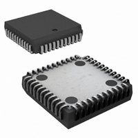
IC DATA AQUIS SYS 12BIT 44-PLCC
Manufacturer
National Semiconductor
Type
Data Acquisition System (DAS)r
Datasheet
1.LM12458CIVNOPB.pdf
(36 pages)
Specifications of LM12458CIVX/NOPB
Resolution (bits)
12 b
Sampling Rate (per Second)
140k
Data Interface
Parallel
Voltage Supply Source
Analog and Digital
Voltage - Supply
3 V ~ 5.5 V
Operating Temperature
-40°C ~ 85°C
Mounting Type
Surface Mount
Package / Case
44-PLCC
Lead Free Status / RoHS Status
Lead free / RoHS Compliant
Other names
*LM12458CIVX
*LM12458CIVX/NOPB
LM12458CIVX
*LM12458CIVX/NOPB
LM12458CIVX
Available stocks
Company
Part Number
Manufacturer
Quantity
Price
Company:

Part Number:
LM12458CIVX/NOPB
Manufacturer:
Texas Instruments
Quantity:
10 000


2.0 Internal User-Programmable
Registers
The completion of the short, single-sample auto-zero calibra-
tion generates Interrupt 3.
The completion of a full auto-zero and linearity self-
calibration generates Interrupt 4.
Interrupt 5 is generated when the Sequencer encounters an
instruction that has its Pause bit (Bit 1 in Instruction RAM
“00”) set to “1”.
The LM12(H)454/8 issues Interrupt 6 whenever it senses
that its power supply voltage is dropping below 4V (typ). This
interrupt indicates the potential corruption of data returned
by the LM12(H)454/8.
Interrupt 7 is issued after a short delay (10 ms typ) while the
LM12(H)454/8 returns from Standby mode to active opera-
tion using the Configuration register’s Bit 4. This short delay
allows the internal analog circuitry to settle sufficiently, en-
suring accurate conversion results.
2.4 INTERRUPT ENABLE REGISTER
The Interrupt Enable register at address location 1001
(A4–A1, BW = 0) or 1001x (A4–A0, BW = 1) has READ/
WRITE capability. An individual interrupt’s ability to produce
an external interrupt at pin 31 (INT) is accomplished by
placing a “1” in the appropriate bit location. Any of the
internal interrupt-producing operations will set their corre-
sponding bits to “1” in the Interrupt Status register regardless
of the state of the associated bit in the Interrupt Enable
register. See Section 2.3 for more information about each of
the eight internal interrupts.
Bit 0 enables an external interrupt when an internal “watch-
dog” comparison limit interrupt has taken place.
Bit 1 enables an external interrupt when the Sequencer has
reached the address stored in Bits 8–10 of the Interrupt
Enable register.
Bit 2 enables an external interrupt when the Conversion
FIFO’s limit, stored in Bits 11–15 of the Interrupt Enable
register, has been reached.
Bit 3 enables an external interrupt when the single-sample
auto-zero calibration has been completed.
Bit 4 enables an external interrupt when a full auto-zero and
linearity self-calibration has been completed.
Bit 5 enables an external interrupt when an internal Pause
interrupt has been generated.
Bit 6 enables an external interrupt when a low power supply
condition (V
Bit 7 enables an external interrupt when the LM12(H)454/8
return from power-down to active mode.
Bits 8 – 10 form the storage location of the user-
programmable value against which the Sequencer’s address
is compared. When the Sequencer reaches an address that
is equal to the value stored in Bits 8–10, an internal interrupt
is generated and appears in Bit 1 of the Interrupt Status
register. If Bit 1 of the Interrupt Enable register is set to “1”,
an external interrupt will appear at pin 31 (INT).
The value stored in bits 8–10 ranges from 000 to 111,
representing 0 to 7 instructions stored in the Instruction
RAM. After the Instruction RAM has been programmed and
the RESET bit is set to “1”, the Sequencer is started by
placing a “1” in the Configuration register’s START bit. Set-
ting the INT 1 trigger value to 000 does not generate an
INT 1 the first time the Sequencer retrieves and decodes
A
+
<
4V) has generated an internal interrupt.
(Continued)
29
Instruction 000. The Sequencer generates INT 1 (by placing
a “1” in the Interrupt Status register’s Bit 1) the second time
and after the Sequencer encounters Instruction 000. It is
important to remember that the Sequencer continues to
operate even if an Instruction interrupt (INT 1) is internally or
externally generated. The only mechanisms that stop the
Sequencer are an instruction with the PAUSE bit set to “1”
(halts before instruction execution), placing a “0” in the Con-
figuration register’s START bit, or placing a “1” in the Con-
figuration register’s RESET bit.
Bits 11–15 hold the number of conversions that must be
stored in the Conversion FIFO in order to generate an inter-
nal interrupt. This internal interrupt appears in Bit 2 of the
Interrupt Status register. If Bit 2 of the Interrupt Enable
register is set to “1”, an external interrupt will appear at pin
31 (INT).
3.0 Other Registers and Functions
3.1 INTERRUPT STATUS REGISTER
This read-only register is located at address 1010 (A4–A1,
BW = 0) or 1010x (A4–A0, BW = 1). The corresponding flag
in the Interrupt Status register goes high (“1”) any time that
an interrupt condition takes place, whether an interrupt is
enabled or disabled in the Interrupt Enable register. Any of
the active (“1”) Interrupt Status register flags are reset to “0”
whenever this register is read or a device reset is issued
(see Bit 1 in the Configuration Register).
Bit 0 is set to “1” when a “watchdog” comparison limit
interrupt has taken place.
Bit 1 is set to “1” when the Sequencer has reached the
address stored in Bits 8–10 of the Interrupt Enable register.
Bit 2 is set to “1” when the Conversion FIFO’s limit, stored in
Bits 11–15 of the Interrupt Enable register, has been
reached.
Bit 3 is set to “1” when the single-sample auto-zero has been
completed.
Bit 4 is set to “1” when an auto-zero and full linearity self-
calibration has been completed.
Bit 5 is set to “1” when a Pause interrupt has been gener-
ated.
Bit 6 is set to “1” when a low-supply voltage condition
(V
Bit 7 is set to “1” when the LM12(H)454/8 return from
power-down to active mode.
Bits 8–10 hold the Sequencer’s actual instruction address
while it is running.
Bits 11–15 hold the actual number of conversions stored in
the Conversion FIFO while the Sequencer is running.
3.2 LIMIT STATUS REGISTER
The read-only register is located at address 1101 (A4–A1,
BW = 0) or 1101x (A4–A0, BW = 1). This register is used in
tandem with the Limit #1 and Limit #2 registers in the Instruc-
tion RAM. Whenever a given instruction’s input voltage ex-
ceeds the limit set in its corresponding Limit register (#1 or
#2), a bit, corresponding to the instruction number, is set in
the Limit Status register. Any of the active (“1”) Limit Status
flags are reset to “0” whenever this register is read or a
device reset is issued (see Bit 1 in the Configuration regis-
ter). This register holds the status of limits #1 and #2 for each
of the eight instructions.
Bits 0–7 show the Limit #1 status. Each bit will be set high
(“1”) when the corresponding instruction’s input voltage ex-
A
+
<
4V) has taken place.
www.national.com
Related parts for LM12458CIVX/NOPB
Image
Part Number
Description
Manufacturer
Datasheet
Request
R

Part Number:
Description:
A/D Converter (A-D) IC
Manufacturer:
National Semiconductor
Datasheet:

Part Number:
Description:
IC ACQUISITION SYS 12BIT 44-PLCC
Manufacturer:
National Semiconductor
Datasheet:

Part Number:
Description:
12-Bit + Sign Data Acquisition System with Self-Calibration
Manufacturer:
National Semiconductor
Datasheet:
Part Number:
Description:
National Semiconductor [8-Bit D/A Converter]
Manufacturer:
National Semiconductor
Datasheet:
Part Number:
Description:
National Semiconductor [Media Coprocessor]
Manufacturer:
National Semiconductor
Datasheet:
Part Number:
Description:
Digitally Controlled Tone and Volume Circuit with Stereo Audio Power Amplifier, Microphone Preamp Stage and National 3D Sound
Manufacturer:
National Semiconductor
Datasheet:
Part Number:
Description:
Digitally Controlled Tone and Volume Circuit with Stereo Audio Power Amplifier, Microphone Preamp Stage and National 3D Sound
Manufacturer:
National Semiconductor
Datasheet:
Part Number:
Description:
AC97 Rev 2 Codec with Sample Rate Conversion and National 3D Sound
Manufacturer:
National Semiconductor
Part Number:
Description:
Manufacturer:
National Semiconductor
Datasheet:
Part Number:
Description:
Manufacturer:
National Semiconductor
Datasheet:
Part Number:
Description:
General Purpose, Low Voltage, Low Power, Rail-to-Rail Output Operational Amplifiers
Manufacturer:
National Semiconductor
Datasheet:
Part Number:
Description:
8-bit 20 MSPS flash A/D converter.
Manufacturer:
National Semiconductor
Datasheet:
Part Number:
Description:
Low Noise Quad Operational Amplifier
Manufacturer:
National Semiconductor
Datasheet:
Part Number:
Description:
Quad Differential Line Receivers
Manufacturer:
National Semiconductor
Datasheet: