ISL90840WIV2027Z Intersil, ISL90840WIV2027Z Datasheet - Page 6
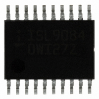
ISL90840WIV2027Z
Manufacturer Part Number
ISL90840WIV2027Z
Description
IC POT DGTL QUAD 10K OHM 20TSSOP
Manufacturer
Intersil
Series
XDCP™r
Datasheet
1.ISL90840WIV2027Z.pdf
(13 pages)
Specifications of ISL90840WIV2027Z
Taps
256
Resistance (ohms)
10K
Number Of Circuits
4
Temperature Coefficient
45 ppm/°C Typical
Memory Type
Volatile
Interface
I²C, 2-Wire Serial
Voltage - Supply
2.7 V ~ 5.5 V
Operating Temperature
-40°C ~ 85°C
Mounting Type
Surface Mount
Package / Case
20-TSSOP
Resistance In Ohms
10K
Lead Free Status / RoHS Status
Lead free / RoHS Compliant
Available stocks
Company
Part Number
Manufacturer
Quantity
Price

Part Number:
ISL90840WIV2027ZT1
Manufacturer:
INTERSIL
Quantity:
20 000


Operating Specifications
NOTES:
10. V
12. MI =
13. Roffset = R
14. RDNL = (R
15. RINL = [R
16. R
17.
18. This parameter is not 100% tested
11.
4. Typical values are for T
5. LSB: [V(R
6. ZS error = V(R
7. FS error = [V(R
8. DNL = [V(R
9. INL = [V(R
SYMBOL
(Note 18)
(Note 18)
(Note 18)
(Note 18)
(Note 18)
t
t
SU:STO
HD:STO
t
t
incremental voltage when changing from one tap to an adjacent tap.
Roffset = R
TC
TC
SU:A
HD:A
Rpu
t
Cb
MATCH
DH
MATCH
t
t
R
F
R
V
|
R
=
=
255
--------------------------------------------------------------- -
[
--------------------------------------------------------------------------------------------- -
[
= [V(R
Max V RW
= (R
Max Ri
[
W
i
W
STOP condition setup time
STOP condition hod time for read, or
volatile only write
Output data hold time
SDA and SCL rise time
SDA and SCL fall time
Capacitive loading of SDA or SCL
SDA and SCL bus pull-up resistor off-
chip
A2, A1 and A0 setup time
A2, A1 and A0 hold time
Max Ri
Max V RW
– (MI • i) – R
i
0
255
W
– R
)
– R
)
/
255
MI, when measuring between R
i
)
i,x
(
i
(
– i • LSB – V(R
W
/
0
MI, when measuring between R
W
– V(R
(
(
W
i-1
|
– R
– V(R
)
(
/
)
0
255. R
)
x)
)
255
(
/
/
+
LSB.
) Min Ri
MI-1, for i = 32 to 255.
i
i,y
–
– V(R
Min Ri
W
)
)
– V
W
PARAMETER
i
/
)
A
)
)
MI, for i = 0 to 255, x = 0 to 3 and y = 0 to 3.
0
i-1
255
i
)
+
) Min V RW
]
(
0
= 25°C and 3.3V supply voltage.
CC
/
]
–
MI, for i = 32 to 255.
]
(
W
Min V RW
/
/
LSB-1, for i = 1 to 255. i is the DCP register setting.
255. V(R
and R
y)
)
]
/
] 2 ⁄
6
LSB.
W
)
i
]
(
]
/
Over the recommended operating conditions unless otherwise specified. (Continued)
)]/LSB for i = 1 to 255.
LSB, for i = 0 to 255, x = 0 to 3 and y = 0 to 3.
(
(
×
0
(
---------------- -
145°C
are the measured resistances for the DCP register set to FF hex and 00 hex respectively.
W
10
)
)
255
i
6
)
)
i
] 2 ⁄
)
and V(R
for i = 32 to 255, T = -40°C to +105°C. Max( ) is the maximum value of the resistance and Min ( ) is
the minimum value of the resistance over the temperature range.
×
W
---------------- -
145°C
W
and R
10
and R
From 30% to 70% of V
From 70% to 30% of V
Total on-chip and off-chip
Before START condition
After STOP condition
From SCL rising edge crossing 70% of V
to SDA rising edge crossing 30% of V
From SDA rising edge to SCL falling edge;
both crossing 70% of V
From SCL falling edge crossing 30% of V
until SDA enters the 30% to 70% of V
window
Maximum is determined by t
For Cb = 400pF, max is about 2~2.5kΩ.
For Cb = 40pF, max is about 15~20kΩ
6
W
)
L
for i = 16 to 240 decimal, T = -40°C to +105°C. Max( ) is the maximum value of the wiper
0
voltage and Min ( ) is the minimum value of the wiper voltage over the temperature range.
.
are V(R
H
.
ISL90840
TEST CONDITIONS
W
) for the DCP register set to FF hex and 00 hex respectively. LSB is the
CC
CC
CC
R
and t
F
CC
CC
CC
CC
,
,
0.1 * Cb
0.1 * Cb
20 +
20 +
MIN
600
600
600
600
10
0
1
(NOTE 4)
TYP
MAX
250
250
400
November 14, 2006
UNIT
FN8086.2
kΩ
pF
ns
ns
ns
ns
ns
ns
ns
Related parts for ISL90840WIV2027Z
Image
Part Number
Description
Manufacturer
Datasheet
Request
R

Part Number:
Description:
Intersil Corporation [CMOS Serial Controller Interface]
Manufacturer:
Intersil Corporation
Datasheet:
Part Number:
Description:
Manufacturer:
Intersil Corporation
Datasheet:
Part Number:
Description:
357-036-542-201 CARDEDGE 36POS DL .156 BLK LOPRO
Manufacturer:
Intersil Corporation
Datasheet:
Part Number:
Description:
1024-Word x 4-Bit LSI Static RAM
Manufacturer:
Intersil Corporation
Datasheet:
Part Number:
Description:
General Purpose NPN Transistor Arrays FN341.4
Manufacturer:
Intersil Corporation
Datasheet:
Part Number:
Description:
CMOS 16-Bit Microprocessor
Manufacturer:
Intersil Corporation
Datasheet:
Part Number:
Description:
Manufacturer:
Intersil Corporation
Datasheet:
Part Number:
Description:
Manufacturer:
Intersil Corporation
Datasheet:
Part Number:
Description:
Manufacturer:
Intersil Corporation
Datasheet:
Part Number:
Description:
Manufacturer:
Intersil Corporation
Datasheet:
Part Number:
Description:
CMOS 6-Bit Latch and Decoder Memory Interfaces
Manufacturer:
Intersil Corporation
Datasheet:
Part Number:
Description:
CA3046General Purpose NPN Transistor Arrays
Manufacturer:
Intersil Corporation
Datasheet:
Part Number:
Description:
Manufacturer:
Intersil Corporation
Datasheet:
Part Number:
Description:
TR909 DLC/FLC SLIC with Low Power Standby
Manufacturer:
Intersil Corporation
Datasheet:
Part Number:
Description:
Manufacturer:
Intersil Corporation
Datasheet: