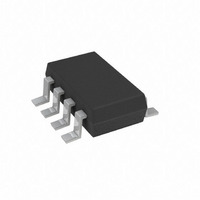
AD5165BUJZ100-R2 Analog Devices Inc, AD5165BUJZ100-R2 Datasheet

AD5165BUJZ100-R2
Specifications of AD5165BUJZ100-R2
AD5165BUJZ100-R2TR
Available stocks
Related parts for AD5165BUJZ100-R2
AD5165BUJZ100-R2 Summary of contents
Page 1
FEATURES Ultralow standby power typical DD 256-position End-to-end resistance 100 kΩ Logic high voltage 1.8 V Power supply 2 5.5 V Low temperature coefficient 35 ppm/°C Compact thin 8-lead TSOT-8 (2.9 mm × 2.8 ...
Page 2
AD5165 TABLE OF CONTENTS Electrical Characteristics—100 kΩ Version .................................. 3 Absolute Maximum Ratings............................................................ 5 Pin Configuration and Functional Descriptions.......................... 6 Typical Performance Characteristics ............................................. 7 Test Circuits..................................................................................... 11 3-Wire Digital Interface................................................................. 12 Theory of Operation ...................................................................... 13 Programming the Variable ...
Page 3
ELECTRICAL CHARACTERISTICS—100 kΩ VERSION ± 10 ± 10 Table 1. Parameter DC CHARACTERISTICS—RHEOSTAT MODE 2 Resistor Differential Nonlinearity 2 Resistor Integral Nonlinearity 3 Nominal Resistor Tolerance Resistance ...
Page 4
AD5165 TIMING CHARACTERISTICS—100 kΩ VERSION ± 10 ± 10 Table 2. Parameter 3-WIRE INTERFACE TIMING CHARACTERISTICS Clock Frequency Input Clock Pulse Width Data Setup Time Data Hold Time ...
Page 5
AD5165 ABSOLUTE MAXIMUM RATINGS +25°C, unless otherwise noted. A Table 3. Parameter V to GND GND Maximum Current Pulsed ...
Page 6
AD5165 PIN CONFIGURATION AND FUNCTIONAL DESCRIPTIONS Table 4. Pin Name Description 1 W Wiper terminal. GND ≤ Positive Power Supply GND Digital Ground. 4 CLK Serial Clock Input. Positive-edge triggered. 5 SDI Serial Data Input ...
Page 7
TYPICAL PERFORMANCE CHARACTERISTICS 0.5 0.4 0.3 0.2 0.1 0 –0.1 –0.2 –0.3 –0.4 –0 128 160 CODE (Decimal) Figure 5. R-INL vs. Code vs. Supply Voltages 0.5 0.4 0.3 0.2 0.1 0 –0.1 –0.2 –0.3 –0.4 ...
Page 8
AD5165 0.5 0.4 0.3 0.2 0.1 0 –0.1 –0.2 –0.3 –0.4 –0 128 160 CODE (Decimal) Figure 11. R-INL vs. Code vs. Temperature, V 0.5 0.4 0.3 0.2 0.1 0 –0.1 –0.2 –0.3 –0.4 –0.5 0 ...
Page 9
100 2. 0.1 0. (1MHz) (V) IH Figure 17. Supply Current vs. Digital Input Voltage –5 –10 ...
Page 10
AD5165 800 700 600 500 400 300 CODE 55 200 CODE FF H 100 0 10k 100k 1M FREQUENCY (Hz) Figure 23. I vs. Frequency 200mV 100ns ...
Page 11
TEST CIRCUITS Figure 27 to Figure 33 illustrate the test circuits that define the test conditions used in the product specification tables DUT 1LSB = V+/ Figure 27. Test Circuit for ...
Page 12
AD5165 3-WIRE DIGITAL INTERFACE Note that in the AD5165 data is loaded MSB first. Table 5. AD5165 Serial Data-Word Format MSB SDI (DATA IN CLK ...
Page 13
AD5165 THEORY OF OPERATION The AD5165 is a 256-position digitally controlled variable resistor (VR) device. PROGRAMMING THE VARIABLE RESISTOR Rheostat Operation The nominal resistance of the RDAC between terminals A and B is available in 100 kΩ. The nominal resistance ...
Page 14
AD5165 PROGRAMMING THE POTENTIOMETER DIVIDER Voltage Output Operation The digital potentiometer easily generates a voltage divider at wiper-to-B and wiper-to-A proportional to the input voltage Unlike the polarity GND, which must be DD ...
Page 15
LAYOUT AND POWER SUPPLY BYPASSING It is good practice to employ compact, minimum lead length layout design. The leads to the inputs should be as direct as possible with a minimum conductor length. Ground paths should have low resistance and ...
Page 16
... AD5165 OUTLINE DIMENSIONS INDICATOR 0.10 MAX ORDERING GUIDE Model R (Ω) Temperature AB AD5165BUJZ100-R2 1 100 k –40°C to +125°C 1 AD5165BUJZ100-R7 100 k –40°C to +125°C AD5165EVAL Pb-free part. © 2004 Analog Devices, Inc. All rights reserved. Trademarks and registered trademarks are the property of their respective owners. ...


