ISL22426UFV14Z-TK Intersil, ISL22426UFV14Z-TK Datasheet - Page 6
ISL22426UFV14Z-TK
Manufacturer Part Number
ISL22426UFV14Z-TK
Description
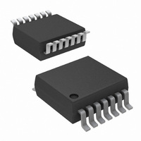
IC POT DGTL 128TP LN LP 14-TSSOP
Manufacturer
Intersil
Series
XDCP™r
Datasheet
1.ISL22426WFR16Z.pdf
(15 pages)
Specifications of ISL22426UFV14Z-TK
Taps
128
Resistance (ohms)
50K
Number Of Circuits
2
Temperature Coefficient
80 ppm/°C Typical
Memory Type
Non-Volatile
Interface
SPI, 3-Wire Serial
Voltage - Supply
2.7 V ~ 5.5 V
Operating Temperature
-40°C ~ 125°C
Mounting Type
Surface Mount
Package / Case
14-TSSOP
Resistance In Ohms
50K
Lead Free Status / RoHS Status
Lead free / RoHS Compliant
Available stocks
Company
Part Number
Manufacturer
Quantity
Price
Company:

Part Number:
ISL22426UFV14Z-TK
Manufacturer:
INTERSIL
Quantity:
340


Operating Specifications
NOTES:
10. INL = [V(RW)
12.
13. MI =
14. Roffset = RW
15. RDNL = (RW
16. RINL = [RW
17. R
18.
19. t
20. Rpu is specified for the highest data rate transfer for the device. Higher value pull-up can be used at lower data rates.
21. Limits should be considered typical and are not production tested.
22. Parameters with MIN and/or MAX limits are 100% tested at +25°C, unless otherwise specified. Temperature limits established by characterization
11. V
5. Typical values are for T
6. LSB: [V(R
7. ZS error = V(RW)
8. FS error = [V(RW)
9. DNL = [V(RW)
SYMBOL
TC
incremental voltage when changing from one tap to an adjacent tap.
TC
hex respectively.
Roffset = RW
and are not production tested.
WC
t
t
MATCH
FO
CS
MATCH
R
V
is the time from the end of a Write sequence of SPI serial interface, to the end of the self-timed internal non-volatile write cycle.
|
=
RW
=
--------------------------------------------------------------- -
[
--------------------------------------------------------------------------------------------- -
[
Max Ri
= [V(RWx)
Max V RW
127
= (RW
[
W
Max Ri
SDO Output Fall Time
CS Deselect Time
Max V RW
)
i
127
i
– (MI • i) – RW
i
– RW
0
127
(
(
– RW
i
– i • LSB – V(RW)]/LSB for i = 1 to 127
/
MI, when measuring between RW and RL.
(
– V(RW)
(
i,x
– V(R
(
/
)
MI, when measuring between RW and RH.
0
(
127
– RW
+
) Min Ri
/
0
LSB.
i
–
|
i-1
Min Ri
– V(RWy)
/
127. MI is a minimum increment. RW
)
)
W
– V
PARAMETER
i
/
)
)
A
MI, for i = 1 to 127.
i
i,y
i-1
)
+
(
) Min V RW
0
= +25°C and 3.3V supply voltage.
CC
(
–
]
)
Min V RW
]
/
/
/
127. V(R
LSB-1, for i = 1 to 127. i is the DCP register setting.
MI, for i = 1 to 127, x = 0 or 1 and y = 0 or 1.
0
)
]
] 2 ⁄
]
)
/
LSB.
/
6
]
MI, for i = 1 to 127.
i
(
]
Over the recommended operating conditions, unless otherwise specified. (Continued)
/
(
LSB, for i = 1 to 127, x = 0 or 1 and y = 0 or 1.
×
(
(
-------------------- -
+165°C
W
10
)
)
127
i
)
6
)
i
] 2 ⁄
)
and V(R
for i = 16 to 112, T = -40°C to +125°C. Max( ) is the maximum value of the resistance and Min ( ) is
the minimum value of the resistance over the temperature range.
×
-------------------- -
+165°C
10
R
W
6
pu
)
0
= 2k, Cb = 30pF
for i = 16 to 112 decimal, T = -40°C to +125°C. Max( ) is the maximum value of the wiper
are V(R
voltage and Min ( ) is the minimum value of the wiper voltage over the temperature range.
127
and RW
ISL22426
TEST CONDITIONS
W
) for the DCP register set to 7F hex and 00 hex respectively. LSB is the
0
are the measured resistances for the DCP register set to 7F hex and 00
(Note 22)
MIN
2
(Note 5)
TYP
(Note 22)
MAX
60
September 8, 2009
UNIT
FN6180.2
ns
µs
Related parts for ISL22426UFV14Z-TK
Image
Part Number
Description
Manufacturer
Datasheet
Request
R

Part Number:
Description:
Intersil Corporation [CMOS Serial Controller Interface]
Manufacturer:
Intersil Corporation
Datasheet:
Part Number:
Description:
Manufacturer:
Intersil Corporation
Datasheet:
Part Number:
Description:
357-036-542-201 CARDEDGE 36POS DL .156 BLK LOPRO
Manufacturer:
Intersil Corporation
Datasheet:
Part Number:
Description:
1024-Word x 4-Bit LSI Static RAM
Manufacturer:
Intersil Corporation
Datasheet:
Part Number:
Description:
General Purpose NPN Transistor Arrays FN341.4
Manufacturer:
Intersil Corporation
Datasheet:
Part Number:
Description:
CMOS 16-Bit Microprocessor
Manufacturer:
Intersil Corporation
Datasheet:
Part Number:
Description:
Manufacturer:
Intersil Corporation
Datasheet:
Part Number:
Description:
Manufacturer:
Intersil Corporation
Datasheet:
Part Number:
Description:
Manufacturer:
Intersil Corporation
Datasheet:
Part Number:
Description:
Manufacturer:
Intersil Corporation
Datasheet:
Part Number:
Description:
CMOS 6-Bit Latch and Decoder Memory Interfaces
Manufacturer:
Intersil Corporation
Datasheet:
Part Number:
Description:
CA3046General Purpose NPN Transistor Arrays
Manufacturer:
Intersil Corporation
Datasheet:
Part Number:
Description:
Manufacturer:
Intersil Corporation
Datasheet:
Part Number:
Description:
TR909 DLC/FLC SLIC with Low Power Standby
Manufacturer:
Intersil Corporation
Datasheet:
Part Number:
Description:
Manufacturer:
Intersil Corporation
Datasheet: