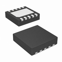
ISL22317UFRTZ Intersil, ISL22317UFRTZ Datasheet - Page 12

ISL22317UFRTZ
Manufacturer Part Number
ISL22317UFRTZ
Description
IC POT DGTL 128TP LN LP 10-TDFN
Manufacturer
Intersil
Series
XDCP™r
Datasheet
1.ISL22317TFRTZ-TK.pdf
(15 pages)
Specifications of ISL22317UFRTZ
Taps
128
Resistance (ohms)
50K
Number Of Circuits
1
Memory Type
Non-Volatile
Interface
I²C, 2-Wire Serial
Voltage - Supply
2.7 V ~ 5.5 V
Operating Temperature
-40°C ~ 125°C
Mounting Type
Surface Mount
Package / Case
10-TDFN Exposed Pad
Resistance In Ohms
50K
Lead Free Status / RoHS Status
Lead free / RoHS Compliant
Temperature Coefficient
-
Available stocks
Company
Part Number
Manufacturer
Quantity
Price
Company:
Part Number:
ISL22317UFRTZ-TK
Manufacturer:
Intersil
Quantity:
50
non-precision DCP by setting this bit to 1. Default value of
the Precision Off bit is 0, i.e. matching to external resistor is
ON.
Note, if the external resistor between REF_A/REF_B is not
populated, the DCP will work as a normal DCP without
giving 99% precision and with ~40% higher value of the
resistance. It is highly recommended to use the bit option
(MSR<6>) to turn OFF the precision mode first and then
removing the external resistor.
All other bits MSR<5:0> are reserved and cannot be written.
Any value read from these bits should be ignored.
I
The ISL22317 supports an I
protocol. The protocol defines any device that sends data
onto the bus as a transmitter and the receiving device as the
receiver. The device controlling the transfer is a master and
the device being controlled is the slave. The master always
initiates data transfers and provides the clock for both
transmit and receive operations. Therefore, the ISL22317
operates as a slave device in all applications.
All communication over the I
sending the MSB of each byte of data first.
Protocol Conventions
Data states on the SDA line must change only during SCL
LOW periods. SDA state changes during SCL HIGH are
reserved for indicating START and STOP conditions (see
Figure 21). On power-up of the ISL22317, the SDA pin is in
the input mode.
2
C Serial Interface
SDA
SCL
2
2
12
C bi-directional bus oriented
C interface is conducted by
FIGURE 21. VALID DATA CHANGES, START, AND STOP CONDITIONS
START
STABLE
DATA
ISL22317
CHANGE
DATA
All I
condition, which is a HIGH to LOW transition of SDA while
SCL is HIGH. The ISL22317 continuously monitors the SDA
and SCL lines for the START condition and does not
respond to any command until this condition is met (see
Figure 21). A START condition is ignored during the
power-up of the device.
All I
condition, which is a LOW to HIGH transition of SDA while
SCL is HIGH (see Figure 21). A STOP condition at the end
of a read operation, or at the end of a write operation, places
the device in its standby mode.
An ACK, Acknowledge, is a software convention used to
indicate a successful data transfer. The transmitting device,
either master or slave, releases the SDA bus after
transmitting eight bits. During the ninth clock cycle, the
receiver pulls the SDA line LOW to acknowledge the
reception of the eight bits of data (see Figure 22).
The ISL22317 responds with an ACK after recognition of a
START condition followed by a valid Identification Byte, and
once again after successful receipt of an Address Byte. The
ISL22317 also responds with an ACK after receiving a Data
Byte of a write operation. The master must respond with an
ACK after receiving a Data Byte of a read operation
A valid Identification Byte contains 01010 as the five MSBs,
and the following bit matching the logic value present at pin
A1. The LSB is the Read/Write bit. Its value is “1” for a Read
operation, and “0” for a Write operation (See Table 4).
(MSB)
0
2
2
C interface operations must begin with a START
C interface operations must be terminated by a STOP
STABLE
DATA
TABLE 4. IDENTIFICATION BYTE FORMAT
1
0
1
STOP
Logic value at pin A1
0
A1
0
April 15, 2010
FN6912.1
(LSB)
R/W


