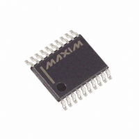
DS1867E-010+T&R Maxim Integrated Products, DS1867E-010+T&R Datasheet - Page 2

DS1867E-010+T&R
Manufacturer Part Number
DS1867E-010+T&R
Description
IC POT W/EEPROM DUAL 10K 20TSSOP
Manufacturer
Maxim Integrated Products
Datasheet
1.DS1867S-10.pdf
(14 pages)
Specifications of DS1867E-010+T&R
Taps
256
Resistance (ohms)
10K
Number Of Circuits
2
Temperature Coefficient
750 ppm/°C Typical
Memory Type
Non-Volatile
Interface
3-Wire Serial
Voltage - Supply
4.5 V ~ 5.5 V
Operating Temperature
-40°C ~ 85°C
Mounting Type
Surface Mount
Package / Case
20-TSSOP
Resistance In Ohms
10K
Lead Free Status / RoHS Status
Lead free / RoHS Compliant
DS1867
DESCRIPTION
The DS1867 Dual Digital Potentiometer with EEPROM is the nonvolatile version of the popular DS1267
Dual Digital Potentiometer. The DS1867 consists of two digitally controlled potentiometers having 256-
position wiper settings. Wiper position is maintained in the absence of power through the use of
EEPROM memory cell arrays. Communication and control of the device are accomplished over a 3-wire
serial port which allows reads and writes of the wiper position. Both potentiometers can be stacked for
increased total resistance with the same resolution. For multiple-device, single-processor environments,
the DS1867 can be cascaded for control over a single 3-wire bus. The DS1867 is offered in three standard
resistance values.
OPERATION
The DS1867 contains two 256-position potentiometers whose wiper positions are set by an 8-bit value.
These two 8-bit values are written to a 17-bit I/O shift register which is used to store wiper position and
the stack select bit when the device is powered. An additional memory area, the shadow memory, stores
the 17-bit I/O shift register during a power-down sequence which provides for wiper nonvolatility. A
block diagram of the DS1867 is presented in Figure 1.
Communication and control of the DS1867 is accomplished through a 3-wire serial port interface that
drives an internal control logic unit. The 3-wire serial interface consists of the three input signals:
,
RST
CLK, and DQ.
The
control signal is used to enable 3-wire serial port operation of the device. The
signal is an
RST
RST
active high input and is required to begin any communication to the DS1867. The CLK signal input is
used to provide timing synchronization for data input and output. The DQ signal line is used to transmit
potentiometer wiper settings and the stack select bit configuration to the 17-bit I/O shift register of the
DS1867.
Figure 2(a) presents the 3-wire serial port protocol. As shown, the 3-wire port is inactive when the
RST
signal input is low. Communication with the DS1867 requires the transition of the
input from a low
RST
state to a high state. Once the 3-wire port has been activated, data is latched into the part on the low to
high transition of the CLK signal input. Three-wire serial timing requirements are provided in the timing
diagrams of Figure 2(b) and (c).
Data written to the DS1867 over the 3-wire serial interface is stored in the 17-bit I/O shift register (see
Figure 3). The 17-bit I/O shift register contains both 8-bit potentiometer wiper position values and the
stack select bit. The composition of the I/O shift register is presented in Figure 3. Bit 0 of the I/O shift
register contains the stack select bit. This bit will be discussed in the section entitled Stacked
Configuration. Bits 1 through 8 of the I/O shift register contain the potentiometer-1 wiper position value.
Bit 1 will contain the MSB of the wiper setting for potentiometer-1 and bit 8 the LSB for the wiper
setting. Bits 9 through 16 of the I/O shift register contain the value of the potentiometer-0 wiper position
with the MSB for the wiper position occupying bit 9 and the LSB bit 16.
2 of 14
102199


