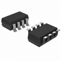
AD5273BRJ50-R2 Analog Devices Inc, AD5273BRJ50-R2 Datasheet - Page 18

AD5273BRJ50-R2
Manufacturer Part Number
AD5273BRJ50-R2
Description
IC DGTL POT 50K 64POS SOT23-8
Manufacturer
Analog Devices Inc
Datasheet
1.AD5273BRJZ10-R7.pdf
(24 pages)
Specifications of AD5273BRJ50-R2
Rohs Status
RoHS non-compliant
Taps
64
Resistance (ohms)
50K
Number Of Circuits
1
Temperature Coefficient
300 ppm/°C Typical
Memory Type
Non-Volatile
Interface
I²C, 2-Wire Serial
Voltage - Supply
2.7 V ~ 5.5 V
Operating Temperature
-40°C ~ 105°C
Mounting Type
Surface Mount
Package / Case
SOT-23-8
Resistance In Ohms
50K
For Use With
AD5273EVAL - BOARD EVAL FOR AD5273
Other names
AD5273BRJ50-R2
AD5273BRJ50-R2TR
AD5273BRJ50-R2TR
AD5273
4.
When all data bits have been read or written, a stop con-
dition is established by the master. A stop condition is
defined as a low-to-high transition on the SDA line
while SCL is high. In write mode, the master pulls the
SDA line high during the 10
stop condition, as shown in Figure 42 and Figure 43. In
read mode, the master issues a no acknowledge for the
ninth clock pulse, that is, the SDA line remains high. The
master then brings the SDA line low before the 10
pulse, which goes high to establish a stop condition, as
shown in Figure 44.
A repeated write function gives the user flexibility to
update the RDAC output continuously, except after
permanent programming, when the part is addressed and
receives instructions only once. During the write cycle,
each data byte updates the RDAC output. For example,
after the RDAC has acknowledged its slave address and
instruction bytes, the RDAC output updates after these two
bytes. If another byte is written to the RDAC while it is still
addressed to a specific slave device with the same instruc-
tion, this byte updates the output of the selected slave device.
If different instructions are needed, the write mode must
be started again with a new slave address, instruction, and
data bytes. Similarly, a repeated read function of the RDAC
is also allowed.
th
clock pulse to establish a
th
clock
Rev. H | Page 18 of 24
CONTROLLING TWO DEVICES ON ONE BUS
Figure 45 shows two AD5273 devices on the same serial bus.
Each has a different slave address because the state of each AD0
pin is different. This allows each device to operate independently.
The master device output bus line drivers are open-drain pull-
down in a fully I
MASTER
Figure 45. Two AD5273 Devices on One Bus
2
C-compatible interface.
AD0
AD5273
SDA SCL
R
P
5V
R
AD0
AD5273
SDA SCL
P
5V
SCL
SDA


