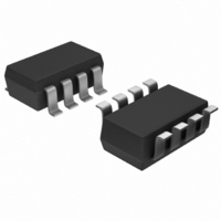
AD5273BRJ50-R2 Analog Devices Inc, AD5273BRJ50-R2 Datasheet - Page 19

AD5273BRJ50-R2
Manufacturer Part Number
AD5273BRJ50-R2
Description
IC DGTL POT 50K 64POS SOT23-8
Manufacturer
Analog Devices Inc
Datasheet
1.AD5273BRJZ10-R7.pdf
(24 pages)
Specifications of AD5273BRJ50-R2
Rohs Status
RoHS non-compliant
Taps
64
Resistance (ohms)
50K
Number Of Circuits
1
Temperature Coefficient
300 ppm/°C Typical
Memory Type
Non-Volatile
Interface
I²C, 2-Wire Serial
Voltage - Supply
2.7 V ~ 5.5 V
Operating Temperature
-40°C ~ 105°C
Mounting Type
Surface Mount
Package / Case
SOT-23-8
Resistance In Ohms
50K
For Use With
AD5273EVAL - BOARD EVAL FOR AD5273
Other names
AD5273BRJ50-R2
AD5273BRJ50-R2TR
AD5273BRJ50-R2TR
APPLICATIONS INFORMATION
DAC
It is common to buffer the output of the digital potentiometer as
a DAC. The buffer minimizes the load dependence and delivers
higher current to the load, if needed.
PROGRAMMABLE VOLTAGE SOURCE WITH
BOOSTED OUTPUT
For applications that require high current adjustment, such as a
laser diode driver or tunable laser, consider a booster voltage
source, as shown in Figure 47.
In this circuit, the inverting input of the op amp forces the
V
ometer. The load current is then delivered by the supply via the
N-Channel FET, N
dissipate (V
imum of 100 mA with a 5 V supply. For precision applications,
a voltage reference, such as the ADR421, ADR03, or ADR370,
can be applied at Terminal A of the digital potentiometer.
PROGRAMMABLE CURRENT SOURCE
A programmable current source can be implemented with the
circuit shown in Figure 48. The load current is the voltage across
Terminal B to Terminal W of the AD5273 divided by R
scale, Terminal A of the AD5273 is −2.048 V, which makes the
wiper voltage clamped at ground potential. Depending on the
load, Equation 5 is therefore valid only at certain codes. For
example, when the compliance voltage, V
the current can be programmed from midscale to full scale of
the AD5273.
OUT
to be equal to the wiper voltage set by the digital potenti-
AD5273
U1
Figure 46. Programmable Voltage Reference (DAC)
Figure 47. Programmable Booster Voltage Source
IN
V
− V
2
1
IN
GND
A
B
V
5V
IN
U1
OUT
ADR03
1
V
. N
W
OUT
) × I
AD8601
1
power handling must be adequate to
3
L
AD5273
+V
U2
–V
power. This circuit can source a max-
U3
U3 2N7002
A W
B
AD8601
5V
SIGNAL
U2
L
, equals half of V
LD
C
C
V
O
R
V
BIAS
OUT
I
L
S
. At zero
REF
Rev. H | Page 19 of 24
,
GAIN CONTROL COMPENSATION
As shown in Figure 49, the digital potentiometers are
commonly used in gain controls or sensor transimpedance
amplifier signal conditioning applications.
In both applications, one of the digital potentiometer terminals
is connected to the op amp inverting node with finite terminal
capacitance, C1. It introduces a zero for the 1 β
20 dB/dec, whereas a typical op amp GBP has −20 dB/dec
characteristics. A large R2 and finite C1 can cause this zero’s
frequency to fall well below the crossover frequency. Therefore,
the rate of closure becomes 40 dB/dec and the system has a 0°
phase margin at the crossover frequency. The output may ring,
or in the worst case, oscillate when the input is a step function.
Similarly, it is also likely to ring when switching between two
gain values because this is equivalent to a step change at the
input. To reduce the effect of C1, users should also configure
Terminal B or Terminal A rather than Terminal W at the
inverting node.
I
L
3
=
2
SLEEP
(
4
GND
V
5V
V
REF191
–2.048 + V
S
REF
Figure 49. Typical Noninverting Gain Amplifier
U1
OUPUT
Figure 48. Programmable Current Source
×
R
S
D
47kΩ
)
L
6
/
R1
64
C1
C1
0V TO ...
|
32
1µF
AD5273
U2
≤
V
OP1177
V–
V+
I
U3
–5V
D
B
+5V
≤
U1
100kΩ
4.7pF
63
R2
C2
W
A
B
W
A
R
R
L
V
S
O
o
102Ω
100Ω
term with
V
L
AD5273
I
L
(5)


