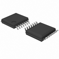
BU2507FV-E2 Rohm Semiconductor, BU2507FV-E2 Datasheet - Page 2

BU2507FV-E2
Manufacturer Part Number
BU2507FV-E2
Description
IC DAC 10BIT 6-CHAN SSOP-B14
Manufacturer
Rohm Semiconductor
Specifications of BU2507FV-E2
Data Interface
Serial
Settling Time
7µs
Number Of Bits
10
Number Of Converters
6
Voltage Supply Source
Single Supply
Operating Temperature
-30°C ~ 85°C
Mounting Type
Surface Mount
Package / Case
14-SSOP
Resolution (bits)
10bit
Sampling Rate
10MSPS
Input Channel Type
Serial
Supply Voltage Range - Analogue
4.5V To 5.5V
Supply Current
850µA
Digital Ic Case Style
SSOP
No. Of
RoHS Compliant
Resolution
10 bit
Interface Type
Serial (3-Wire)
Supply Voltage (max)
5.5 V
Supply Voltage (min)
4.5 V
Maximum Operating Temperature
+ 85 C
Mounting Style
SMD/SMT
Minimum Operating Temperature
- 30 C
Lead Free Status / RoHS Status
Lead free / RoHS Compliant
Power Dissipation (max)
-
Lead Free Status / Rohs Status
Lead free / RoHS Compliant
Other names
BU2507FV-E2
BU2507FV-E2TR
BU2507FV-E2TR
Available stocks
Company
Part Number
Manufacturer
Quantity
Price
Company:
Part Number:
BU2507FV-E2
Manufacturer:
RohmSemic
Quantity:
4 554
Part Number:
BU2507FV-E2
Manufacturer:
ROHM/罗姆
Quantity:
20 000
●Electrical Characteristics (Unless otherwise specified, VCC=5V, VrefH=5V, VrefL=0V, Ta=25℃)
●Timing Characteristics (Unless otherwise specified, VCC=5V, VrefH=5V, VrefL=0V, Ta=25℃)
© 2009 ROHM Co., Ltd. All rights reserved.
BU2508FV,BU2507FV
www.rohm.com
(note) LD signal is level triggered. When LD input is on H level, internal shift-register state is loaded to DAC control latch.
<Digital unit>
<Analog unit>
Power source current
Input leak current
Input voltage L
Input voltage H
Output voltage L
Output voltage H
Consumption current
D/A converter upper standard voltage
setting range
D/A converter lower standard voltage
setting range
Buffer amplifier output voltage range
Buffer amplifier output drive range
Precision
Buffer amplifier output impedance
Pull-up I/O internal resistance value
*1: Value in the case where CH1 ~ CH4 are set to maximum current (after reset)
Reset L pulse width
Clock L pulse width
Clock H pulse width
Clock rise time
Clock fall time
Data setup time
Data hold time
Load setup time
Load hold time
Load H pulse width
DA output settling time
Clock transition during LD=H is inhibited.
Differential non-linearity error
Integral non-linearity error
Zero point error
Full scale error
Parameter
Parameter
Output
RESET
CLK
LD
DI
t
RTL
Symbol
SZERO
Symbol
SFULL
VrefH
tDCH
tCHD
VrefL
tCKH
tCHL
tLDC
tLDH
tLDD
VOH
IrefH
tRTL
tCKL
DNL
VOL
IILK
Rup
ICC
VIH
VIL
INL
RO
VO
tcr
IO
tcf
MIN.
MIN.
12.5
-1.0
-3.5
-25
2.0
4.6
3.0
0.1
0.2
-25
50
50
50
20
40
50
50
50
-5
-2
t
0
0
-
-
-
-
-
-
-
-
CKL
t
DCH
t
cr
2/8
Limits
Limits
TYP.
TYP.
t
0.85
CHD
4.5
2.0
25
5
7
-
-
-
-
-
-
-
-
-
-
-
-
-
-
-
-
-
-
-
-
-
-
-
-
t
CKH
t
CHL
MAX.
MAX.
4.75
37.5
2.8
0.8
0.4
7.5
3.4
1.5
4.9
1.0
3.5
25
25
15
50
50
20
5
5
5
2
t
-
-
-
-
-
-
-
-
-
cf
mA
LSB
Unit
Unit
mA
mA
mA
mV
μA
kΩ
nS
μS
Ω
V
V
V
V
V
V
V
t
LDH
(*1)
t
LDD
At CLK = 10MHz, IAO = 0uA
VIN=0 to VCC
IOL=2.5mA
IOH=-2.5mA
Data condition : at maximum current
Outputs does not necessarily take a
value in standard voltage setting range.
Value that output may take is in the buffer
amplifier output voltage range (VO).
IO=±100μA
IO=±1.0mA
Upper side saturation voltage =0.35V
(on full scale setting, current sourcing )
Lower side saturation voltage =0.23V
(on zero scale setting, current sinking )
VrefH =4.796V
VrefL=0.7V
VCC=5.5V (4mV/LSB)
No load (IO = +0mA)
Input voltage 0V
(Resistance value changes according
to voltage to be impressed.)
Judgment level is 80% / 20% of VCC.
CL≦100pF, VO:0.5V⇔4.5V .
Until output value deference from final
value becomes 1/2LSB
t
LDC
Conditions
Conditions
-
-
-
-
-
-
-
-
-
-
-
-
-
Technical Note
2011.04 - Rev.B


