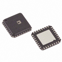
AD9704BCPZ Analog Devices Inc, AD9704BCPZ Datasheet - Page 38

AD9704BCPZ
Manufacturer Part Number
AD9704BCPZ
Description
IC DAC TX 8BIT 175MSPS 32-LFCSP
Manufacturer
Analog Devices Inc
Series
TxDAC®r
Datasheet
1.AD9704BCPZ.pdf
(52 pages)
Specifications of AD9704BCPZ
Data Interface
Serial
Settling Time
11ns
Number Of Bits
8
Number Of Converters
1
Voltage Supply Source
Analog and Digital
Power Dissipation (max)
50mW
Operating Temperature
-40°C ~ 85°C
Mounting Type
Surface Mount
Package / Case
32-LFCSP
Resolution (bits)
8bit
Sampling Rate
175MSPS
Input Channel Type
Parallel
Supply Current
5.1mA
Digital Ic Case Style
CSP
No. Of Pins
32
Supply Voltage Range - Analogue
3.3V To 3.6V
Rohs Compliant
Yes
Number Of Channels
1
Resolution
8b
Interface Type
Parallel
Single Supply Voltage (typ)
1.8/3.3V
Architecture
Segment
Power Supply Requirement
Analog and Digital
Output Type
Current
Integral Nonlinearity Error
±0.09LSB
Single Supply Voltage (min)
1.7V
Single Supply Voltage (max)
3.6V
Operating Temp Range
-40C to 85C
Operating Temperature Classification
Industrial
Mounting
Surface Mount
Pin Count
32
Package Type
LFCSP EP
Lead Free Status / RoHS Status
Lead free / RoHS Compliant
Lead Free Status / RoHS Status
Lead free / RoHS Compliant, Lead free / RoHS Compliant
Available stocks
Company
Part Number
Manufacturer
Quantity
Price
Company:
Part Number:
AD9704BCPZ
Manufacturer:
Analog Devices Inc
Quantity:
135
Company:
Part Number:
AD9704BCPZ
Manufacturer:
FREESCAL
Quantity:
2
Part Number:
AD9704BCPZ
Manufacturer:
ADI/亚德诺
Quantity:
20 000
AD9704/AD9705/AD9706/AD9707
Sleep and Power-Down Operation (Pin Mode)
The AD9704/AD9705/AD9706/AD9707 have a sleep mode
that turns off the output current and reduces the total power
consumed by the device. This mode is activated by applying
a Logic 1 to the SLEEP/CSB pin. The SLEEP/CSB pin logic
threshold is equal to 0.5 × DVDD. This digital input also
contains an active pull-down circuit.
The AD9704/AD9705/AD9706/AD9707 take less than 50 ns to
power down and approximately 5 μs to power back up.
Sleep and Power-Down Operation (SPI Mode)
The AD9704/AD9705/AD9706/AD9707 offer three power-
down functions that can be controlled through the SPI. These
power-down modes can be used to minimize the power
dissipation of the device. The power-down functions are
controlled through SPI Register 0x00, Bit 1 to Bit 3. Table 26
summarizes the power-down functions that can be controlled
through the SPI. The power-down mode can be enabled by
writing a Logic 1 to the corresponding bit in Register 0x00.
Table 26. Power-Down Mode Selection
Power-Down
Mode
Clock Off
Sleep
Power Down
(Reg. 0x00)
Bit Number
1
2
3
Functional Description
Turn off clock
Turn off output current
Turn off output current and
internal band gap reference
Rev. A | Page 38 of 52
SELF-CALIBRATION
The AD9704/AD9705/AD9706/AD9707 have a self-calibration
feature that improves the DNL of the device. Performing a self-
calibration on the device improves device performance in low
frequency applications. The device performance in applications
where the analog output frequencies are above 1 MHz are
generally influenced more by dynamic device behavior than by
DNL, and in these cases, self-calibration is unlikely to provide
any benefits for single-tones, as shown in Figure 87. Figure 88
shows that self-calibration is helpful up to 20 MHz for two-tone
IMD spaced 10 kHz apart.
Figure 87. AD9707 SFDR vs. f
Figure 88. IMD vs. Lower f
88
86
84
82
80
78
88
87
86
85
84
83
82
81
80
79
78
0
0
UNCALIBRATED
UNCALIBRATED
0.2
5
CALIBRATED
CALIBRATED
LOWER
OUT
f
OUT
OUT
@ 175 MSPS and I
@ 175 MSPS and I
0.4
10
f
(MHz)
OUT
(MHz)
0.6
15
OUTFS
OUTFS
= 2 mA
= 2 mA
0.8
20


