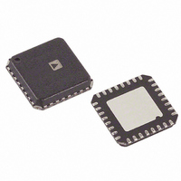
AD9704BCPZ Analog Devices Inc, AD9704BCPZ Datasheet - Page 41

AD9704BCPZ
Manufacturer Part Number
AD9704BCPZ
Description
IC DAC TX 8BIT 175MSPS 32-LFCSP
Manufacturer
Analog Devices Inc
Series
TxDAC®r
Datasheet
1.AD9704BCPZ.pdf
(52 pages)
Specifications of AD9704BCPZ
Data Interface
Serial
Settling Time
11ns
Number Of Bits
8
Number Of Converters
1
Voltage Supply Source
Analog and Digital
Power Dissipation (max)
50mW
Operating Temperature
-40°C ~ 85°C
Mounting Type
Surface Mount
Package / Case
32-LFCSP
Resolution (bits)
8bit
Sampling Rate
175MSPS
Input Channel Type
Parallel
Supply Current
5.1mA
Digital Ic Case Style
CSP
No. Of Pins
32
Supply Voltage Range - Analogue
3.3V To 3.6V
Rohs Compliant
Yes
Number Of Channels
1
Resolution
8b
Interface Type
Parallel
Single Supply Voltage (typ)
1.8/3.3V
Architecture
Segment
Power Supply Requirement
Analog and Digital
Output Type
Current
Integral Nonlinearity Error
±0.09LSB
Single Supply Voltage (min)
1.7V
Single Supply Voltage (max)
3.6V
Operating Temp Range
-40C to 85C
Operating Temperature Classification
Industrial
Mounting
Surface Mount
Pin Count
32
Package Type
LFCSP EP
Lead Free Status / RoHS Status
Lead free / RoHS Compliant
Lead Free Status / RoHS Status
Lead free / RoHS Compliant, Lead free / RoHS Compliant
Available stocks
Company
Part Number
Manufacturer
Quantity
Price
Company:
Part Number:
AD9704BCPZ
Manufacturer:
Analog Devices Inc
Quantity:
135
Company:
Part Number:
AD9704BCPZ
Manufacturer:
FREESCAL
Quantity:
2
Part Number:
AD9704BCPZ
Manufacturer:
ADI/亚德诺
Quantity:
20 000
DIFFERENTIAL BUFFERED OUTPUT
USING AN OP AMP
A dual op amp (see the circuit shown in Figure 91) can be used
in a differential version of the single-ended buffer shown in
Figure 90. The same R-C network is used to form a 1-pole
differential, low-pass filter to isolate the op amp inputs from the
high frequency images produced by the DAC outputs. The feed-
back resistors, R
formula
The maximum and minimum voltages out of the amplifier are,
respectively,
The common-mode voltage of the output is determined by the
formula
V
V
V
V
OUT
MIN
MAX
CM
= V
= R
=
=
V
V
FB
MAX
MAX
REF
× I
FB
− V
, determine the peak signal swing by the
−
×
FS
V
⎛
⎜
⎜
⎝
1
OUT
OUT
2
+
R
R
FB
B
⎞
⎟
⎟
⎠
Rev. A | Page 41 of 52
AD9704/AD9705
AD9706/AD9707
AD9704/AD9705/AD9706/AD9707
IOUTA
IOUTB
REFIO
OTCM
Figure 91. Single-Supply Differential Buffer
21
19
23
20
R
S
R
S
R
C
R
B
B
ADA4841-2
ADA4841-2
–
+
+
–
R
R
C
C
FB
FB
F
F
V
OUT


