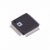
AD9763ASTZ Analog Devices Inc, AD9763ASTZ Datasheet - Page 16

AD9763ASTZ
Manufacturer Part Number
AD9763ASTZ
Description
IC DAC 10BIT DUAL 125MSPS 48LQFP
Manufacturer
Analog Devices Inc
Series
TxDAC+®r
Specifications of AD9763ASTZ
Data Interface
Parallel
Settling Time
35ns
Number Of Bits
10
Number Of Converters
2
Voltage Supply Source
Analog and Digital
Power Dissipation (max)
450mW
Operating Temperature
-40°C ~ 85°C
Mounting Type
Surface Mount
Package / Case
48-LQFP
Resolution (bits)
10bit
Sampling Rate
125MSPS
Input Channel Type
Parallel
Supply Voltage Range - Analog
3V To 5.5V
Supply Voltage Range - Digital
2.7V To 5.5V
Lead Free Status / RoHS Status
Lead free / RoHS Compliant
For Use With
AD9763-EBZ - BOARD EVAL FOR AD9763
Lead Free Status / RoHS Status
Lead free / RoHS Compliant, Lead free / RoHS Compliant
Available stocks
Company
Part Number
Manufacturer
Quantity
Price
Company:
Part Number:
AD9763ASTZ
Manufacturer:
ADI
Quantity:
180
Company:
Part Number:
AD9763ASTZ
Manufacturer:
Analog Devices Inc
Quantity:
10 000
Part Number:
AD9763ASTZ
Manufacturer:
ADI/亚德诺
Quantity:
20 000
Company:
Part Number:
AD9763ASTZRL
Manufacturer:
Analog Devices Inc
Quantity:
10 000
Part Number:
AD9763ASTZRL
Manufacturer:
ADI/亚德诺
Quantity:
20 000
AD9763
Timing specifications for interleaved mode are shown in Figure 28
and Figure 29.
The digital inputs are CMOS compatible with logic thresholds,
V
(DVDD) or
THRESHOLD
INTERLEAVED
DAC OUTPUT
DAC OUTPUT
DATA IN
IQWRT
V
IQCLK
IQSEL
I
I
OUTA
OUTB
THRESHOLD
IQRESET
OR
*APPLIES TO FALLING EDGE OF IQCLK/IQWRT AND IQSEL ONLY.
PORT 1
PORT 2
IQWRT
IQCLK
IQSEL
DATA
, set to approximately half the digital positive supply
= DVDD/2 (±20%)
xx
Figure 28. Interleaved Mode Timing
Figure 29. Interleaved Mode Timing
t
H
*
D1
xx
xx
t
S
D2
t
PD
t
H
D3
t
LPW
D1
D2
D4
D5
D3
D4
Rev. D | Page 16 of 32
The internal digital circuitry of the AD9763 is capable of
operating over a digital supply range of 3.3 V to 5 V. As a result,
the digital inputs can also accommodate TTL levels when DVDD
is set to accommodate the maximum high level voltage of the
TTL drivers V
proper compatibility with most TTL logic families. Figure 30
shows the equivalent digital input circuit for the data and clock
inputs. The sleep mode input is similar with the exception that
it contains an active pull-down circuit, thus ensuring that the
AD9763 remains enabled if this input is left disconnected.
Because the AD9763 is capable of being clocked up to 125 MSPS,
the quality of the clock and data input signals are important in
achieving the optimum performance. Operating the AD9763
with reduced logic swings and a corresponding digital supply
(DVDD) results in the lowest data feedthrough and on-chip
digital noise. The drivers of the digital data interface circuitry
should be specified to meet the minimum setup and hold times
of the AD9763 as well as its required minimum/maximum
input logic level thresholds.
Digital signal paths should be kept short and run lengths matched
to avoid propagation delay mismatch. The insertion of a low
value resistor network (20 Ω to 100 Ω) between the AD9763
digital inputs and driver outputs can be helpful in reducing any
overshooting and ringing at the digital inputs that contribute to
digital feedthrough. For longer board traces and high data
update rates, stripline techniques with proper impedance and
termination resistors should be considered to maintain clean
digital inputs.
The external clock driver circuitry should provide the AD9763
with a low jitter clock input meeting the minimum/maximum
logic levels while providing fast edges. Fast clock edges help
minimize any jitter that manifests itself as phase noise on a
reconstructed waveform. Thus, the clock input should be driven
by the fastest logic family suitable for the application.
Note that the clock input can also be driven via a sine wave that
is centered around the digital threshold (DVDD/2) and meets
the min/max logic threshold. This typically results in a slight
degradation in the phase noise, and becomes more noticeable at
higher sampling rates and output frequencies. Also, at higher
sampling rates, the 20% tolerance of the digital logic threshold
should be considered because it affects the effective clock duty
cycle and, subsequently, cuts into the required data setup and
hold times.
OH(MAX)
DIGITAL
INPUT
Figure 30. Equivalent Digital Input
. A DVDD of 3.3 V typically ensures
DVDD


