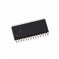
HI5731BIB Intersil, HI5731BIB Datasheet - Page 12

HI5731BIB
Manufacturer Part Number
HI5731BIB
Description
IC DAC 12-BIT 100MSPS 28-SOIC
Manufacturer
Intersil
Datasheet
1.HI5731BIB.pdf
(17 pages)
Specifications of HI5731BIB
Settling Time
20ns
Number Of Bits
12
Data Interface
Parallel
Number Of Converters
1
Voltage Supply Source
Analog and Digital, Dual ±
Power Dissipation (max)
650mW
Operating Temperature
-40°C ~ 85°C
Mounting Type
Surface Mount
Package / Case
28-SOIC (7.5mm Width)
Lead Free Status / RoHS Status
Contains lead / RoHS non-compliant
Available stocks
Company
Part Number
Manufacturer
Quantity
Price
Company:
Part Number:
HI5731BIB
Manufacturer:
HARRIS
Quantity:
37
Part Number:
HI5731BIB
Manufacturer:
H
Quantity:
20 000
Part Number:
HI5731BIBZ
Manufacturer:
INTERSIL
Quantity:
20 000
Interfacing to the HSP45106 NCO-16
The HSP45106 is a 16-bit, Numerically Controlled Oscillator
(NCO). The HSP45106 can be used to generate various
modulation schemes for Direct Digital Synthesis (DDS)
applications. Figure 28 shows how to interface an HI5731 to
the HSP45106.
Interfacing to the HSP45102 NCO-12
The HSP45102 is a 12-bit, Numerically Controlled Oscillator
(NCO). The HSP45102 can be used to generate various
modulation schemes for Direct Digital Synthesis (DDS)
applications. Figure 29 shows how to interface an HI5731 to
the HSP45102.
This high level block diagram is that of a basic PSK
modulator. In this example the encoder generates the PSK
waveform by driving the Phase Modulation Inputs (P1, P0) of
the HSP45102. The P1-0 inputs impart a phase shift to the
carrier wave as defined in Table 2.
The data port of the HSP45102 drives the 12-bit HI5731
DAC which converts the NCO output into an analog
waveform. The output filter connected to the DAC can be
tailored to remove unwanted spurs for the desired carrier
frequency. The controller is used to load the desired center
frequency and control the HSP45102. The HI5731 coupled
with the HSP45102 make an inexpensive PSK modulator
with Spurious Free performance down to -76dBc.
Definition of Specifications
Integral Linearity Error, INL, is the measure of the worst
case point that deviates from a best fit straight line of data
values along the transfer curve.
Differential Linearity Error, DNL, is the measure of the
error in step size between adjacent codes along the
converter’s transfer curve. Ideally, the step size is 1 LSB from
one code to the next, and the deviation from 1 LSB is known
as DNL. A DNL specification of greater than -1 LSB
guarantees monotonicity.
Feedthru, is the measure of the undesirable switching noise
coupled to the output.
Output Voltage Full Scale Settling Time, is the time
required from the 50% point on the clock input for a full scale
step to settle within an ±
Output Voltage Small Scale Settling Time, is the time
required from the 50% point on the clock input for a 100mV
P1
0
0
1
1
TABLE 3. PHASE MODULATION INPUT CODING
P0
0
1
0
1
1
/
2
LSB error band.
PHASE SHIFT (DEGREES)
12
270
180
90
0
HI5731
step to settle within an
applications reconstructing highly correlated signals such as
sine waves with more than 5 points per cycle.
Glitch Area, GE, is the switching transient appearing on the
output during a code transition. It is measured as the area
under the curve and expressed as a picoVolt-time
specification (typically pV-s).
Differential Gain, ∆A
wave with a normalized amplitude.
Differential Phase, ∆Φ, is the phase error from an ideal sine
wave.
Signal to Noise Ratio, SNR, is the ratio of a fundamental to
the noise floor of the analog output. The first 5 harmonics
are ignored, and an output filter of
used to eliminate alias products.
Total Harmonic Distortion, THD, is the ratio of the DAC
output fundamental to the RMS sum of the harmonics. The
first 5 harmonics are included, and an output filter of
clock frequency is used to eliminate alias products.
Spurious Free Dynamic Range, SFDR, is the amplitude
difference from a fundamental to the largest harmonically or
non-harmonically related spur. A sine wave is loaded into the
D/A and the output filtered at
eliminate noise from clocking alias terms.
Intermodulation Distortion, IMD, is the measure of the
sum and difference products produced when a two tone
input is driven into the D/A. The distortion products created
will arise at sum and difference frequencies of the two tones.
IMD can be calculated using the following equation:
IMD
=
20Log (RMS of Sum and Difference Distortion Products)
------------------------------------------------------------------------------------------------------------------------------------------------------ - .
(
RMS Amplitude of the Fundamental
V
, is the gain error from an ideal sine
1
/
2
LSB error band. This is used by
1
/
2
the clock frequency to
1
/
2
the clock frequency is
)
1
/
2
the


