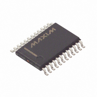
MAX5590BEUG+ Maxim Integrated Products, MAX5590BEUG+ Datasheet - Page 23

MAX5590BEUG+
Manufacturer Part Number
MAX5590BEUG+
Description
IC DAC 12BIT OCTAL BUFF 24-TSSOP
Manufacturer
Maxim Integrated Products
Datasheet
1.MAX5590BEUG.pdf
(33 pages)
Specifications of MAX5590BEUG+
Settling Time
3µs
Number Of Bits
12
Data Interface
Serial
Number Of Converters
8
Voltage Supply Source
Analog and Digital
Operating Temperature
-40°C ~ 85°C
Mounting Type
Surface Mount
Package / Case
24-TSSOP
Resolution
12 bit
Interface Type
Serial (SPI)
Supply Voltage (max)
5.25 V
Supply Voltage (min)
2.7 V
Maximum Operating Temperature
+ 85 C
Mounting Style
SMD/SMT
Minimum Operating Temperature
- 40 C
Supply Current
3.2 mA
Voltage Reference
External
Lead Free Status / RoHS Status
Lead free / RoHS Compliant
Power Dissipation (max)
-
Lead Free Status / Rohs Status
Lead free / RoHS Compliant
DAC Programming Examples:
To load input register A from the shift register, leaving
DAC register A unchanged (DAC output unchanged),
use the command in Table 3.
The MAX5590–MAX5595 can load all of the input regis-
ters (A–H) simultaneously from the shift register, leaving
the DAC registers unchanged (DAC output unchanged),
by using the command in Table 4.
To load all of the input registers (A–H) and all of the DAC
registers (A–H) simultaneously, use the command in
Table 5.
For the 10-bit and 8-bit versions, set sub-bits = 0 for
best performance.
Table 3. Load Input Register A from Shift Register
Table 4. Load Input Registers (A–H) from Shift Register
Table 5. Load Input Registers (A–H) and DAC Registers (A–H) from Shift Register
Table 6. Select Bits (M_)
X = Don’t care.
Table 7. Select Bits Programming Example
X = Don’t care.
DATA
DATA
DATA
DATA
DATA
DIN
DIN
DIN
DIN
DIN
1
1
1
1
0
CONTROL BITS
CONTROL BITS
CONTROL BITS
Buffered, Fast-Settling, Octal, 12/10/8-Bit,
0
0
0
0
0
______________________________________________________________________________________
0
1
0
0
0
CONTROL BITS
CONTROL BITS
1
0
0
0
0
D11
D11
D11
X
X
D10
D10
D10
X
X
D9
D9
D9
X
0
D8
D8
D8
X
0
The select bits allow synchronous updating of any com-
bination of channels. The select bits command the
loading of the DAC register from the input register of
each channel. Set the select bit M_ = 1 to load the DAC
register “_” with data from the input register “_”, where
“_” is replaced with A, B, or C and so on through H,
depending on the selected channel. Setting the select
bit M_ = 0 results in no action for that channel (Table 6).
Select Bits Programming Example:
To load DAC register B from input register B while
keeping other channels (A, C–H) unchanged, set MB =
1 and M_ = 0 (Table 7).
MH
D7
D7
D7
0
Voltage-Output DACs
DATA BITS
DATA BITS
MG
DATA BITS
D6
D6
D6
0
D5
D5
MF
D5
0
Programming Commands
DATA BITS
DATA BITS
ME
D4
D4
D4
0
D3/0
D3/0
D3/0
MD
0
Advanced-Feature
D2/0
D2/0
D2/0
MC
0
Select Bits (M_)
D1/0
D1/0
D1/0
MB
1
D0/0
D0/0
D0/0
MA
0
23


