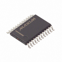
MAX5590BEUG+ Maxim Integrated Products, MAX5590BEUG+ Datasheet - Page 6

MAX5590BEUG+
Manufacturer Part Number
MAX5590BEUG+
Description
IC DAC 12BIT OCTAL BUFF 24-TSSOP
Manufacturer
Maxim Integrated Products
Datasheet
1.MAX5590BEUG.pdf
(33 pages)
Specifications of MAX5590BEUG+
Settling Time
3µs
Number Of Bits
12
Data Interface
Serial
Number Of Converters
8
Voltage Supply Source
Analog and Digital
Operating Temperature
-40°C ~ 85°C
Mounting Type
Surface Mount
Package / Case
24-TSSOP
Resolution
12 bit
Interface Type
Serial (SPI)
Supply Voltage (max)
5.25 V
Supply Voltage (min)
2.7 V
Maximum Operating Temperature
+ 85 C
Mounting Style
SMD/SMT
Minimum Operating Temperature
- 40 C
Supply Current
3.2 mA
Voltage Reference
External
Lead Free Status / RoHS Status
Lead free / RoHS Compliant
Power Dissipation (max)
-
Lead Free Status / Rohs Status
Lead free / RoHS Compliant
Buffered, Fast-Settling, Octal, 12/10/8-Bit,
Voltage-Output DACs
TIMING CHARACTERISTICS—DSP Mode Disabled (3V, 3.3V, 5V Logic) (Figure 1)
(DV
6
SCLK Frequency
SCLK Pulse-Width High
SCLK Pulse-Width Low
CS Fall to SCLK Rise Setup Time
SCLK Rise to CS Rise Hold Time
SCLK Rise to CS Fall Setup
DIN to SCLK Rise Setup Time
DIN to SCLK Rise Hold Time
SCLK Rise to DOUTDC1 Valid
Propagation Delay
SCLK Fall to DOUT_ Valid
Propagation Delay
CS Rise to SCLK Rise Hold Time
CS Pulse-Width High
UPIO_ TIMING CHARACTERISTICS
DOUT Tri-State Time when Exiting
DOUTDC0, DOUTDC1, and UPIO
Modes
DOUTRB Tri-State Time from CS
Rise
DOUTRB Tri-State Enable Time
from 8th SCLK Rise
LDAC Pulse-Width Low
LDAC Effective Delay
CLR, MID, SET Pulse-Width Low
GPO Output Settling Time
GPO Output High-Impedance
Time
DD
_______________________________________________________________________________________
= 2.7V to 5.25V, V
PARAMETER
AGND
= 0V, V
SYMBOL
DGND
f
t
t
t
t
t
t
t
SCLK
t
t
t
DRBZ
t
t
t
t
CSW
t
t
CSH
t
t
DO1
DO2
DOZ
CMS
t
CSS
CS0
CS1
ZEN
LDL
LDS
GPZ
CH
DH
CL
DS
GP
= 0V, T
2.7V < DV
(Note 7)
(Note 7)
C
C
mode
MICROWIRE and SPI modes 0 and 3
C
in high impedance
C
in high impedance
C
UPIO_ driven out of tri-state
Figure 5
Figure 6
Figure 5
Figure 6
L
L
L
L
L
A
= 20pF, UPIO_ = DOUTDC1 mode
= 20pF, UPIO_ = DOUTDC0 or DOUTRB
= 20pF, from end of write cycle to UPIO_
= 20pF, from rising edge of CS to UPIO_
= 20pF, from 8th rising edge of SCLK to
= T
MIN
DD
to T
< 5.25V
CONDITIONS
MAX
, unless otherwise noted.)
MIN
100
20
20
10
10
12
10
45
20
20
5
5
0
TYP
MAX
100
100
100
20
30
30
20
UNITS
MHz
ns
ns
ns
ns
ns
ns
ns
ns
ns
ns
ns
ns
ns
ns
ns
ns
ns
ns
ns


